Worked, not summarised.Every figure plotted.
Converter design problems taken all the way to component values, with the plots that show where the answer comes from and where it stops holding.
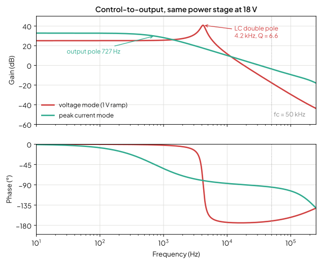
Current mode compensator design
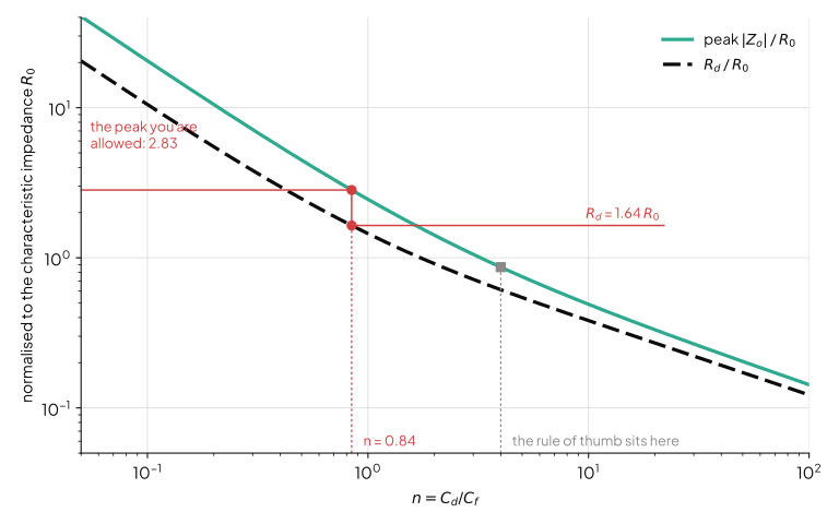
Input Filter Damping: Sizing Rd and Cd to an Impedance Target
Input filter damping sized from the impedance you need: the smallest Rd and Cd that hold a filter's peak under a stated limit, what the resistor dissipates, and where the tolerance goes.
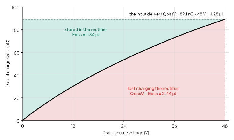
MOSFET Coss Loss in a Half-Bridge: Which Switch Pays, and How Much
MOSFET Coss loss in a hard-switched half-bridge: the switch that turns on pays its own Eoss plus Qoss x V - Eoss for the rectifier, which pays nothing. Worked from a datasheet curve.
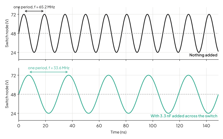
RC Snubber Design: Sizing R and C from a Measured Ring
RC snubber design from a measured ring: find the switch node's parasitic L and C, size the capacitor against its losses, and pick the resistor that damps the ring fastest.
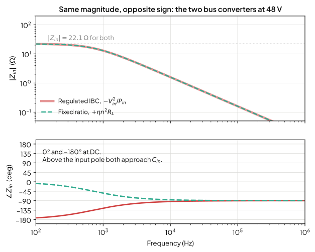
Intermediate Bus Architecture: Regulated or Fixed-Ratio, and What It Costs You
Intermediate bus architecture: a regulated bus converter and an unregulated fixed-ratio one present the same input impedance magnitude, and only one of them peaks at the interface.

Compensator Types: Choosing Between Type I, II and III
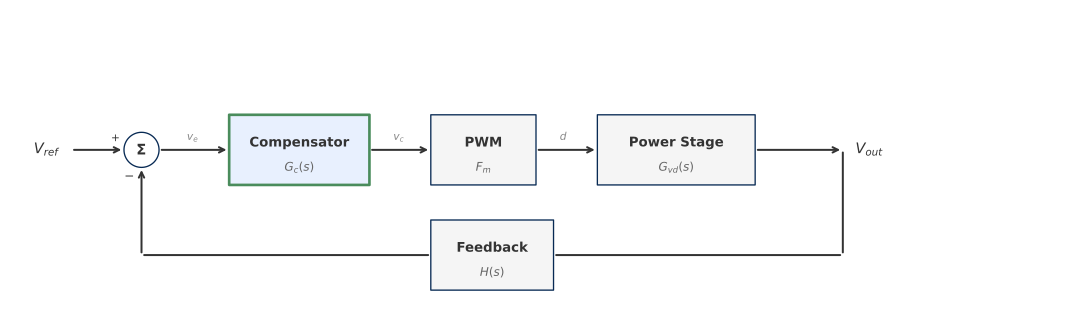
Compensator types explained: how to choose between Type I, II and III from the phase your plant has left at crossover, and why the output capacitor decides it more often than the control mode does.
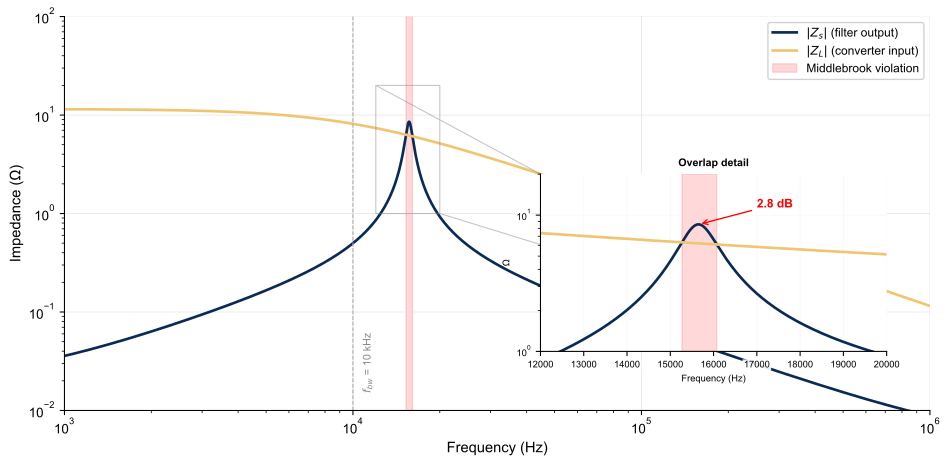
Input filter stability
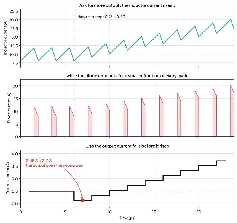
Boost Converter Right-Half-Plane Zero: Why You Can't Compensate Your Way Out
The boost converter's right-half-plane zero: where it comes from, why current-mode control doesn't remove it, and how a bigger inductor can leave your loop with no valid crossover frequency at all.
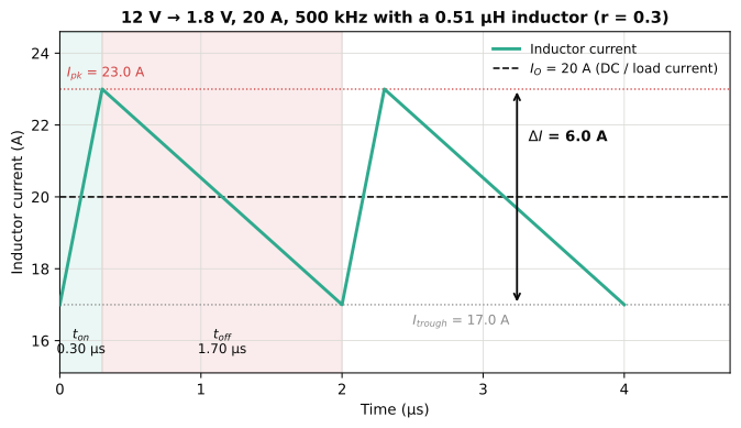
Sizing a Buck Inductor: Ripple Ratio, Saturation and the CCM/DCM Boundary
How to size a buck converter inductor: where the 30% ripple rule comes from, why the loss optimum is a broad basin rather than a number, and why no two manufacturers' saturation ratings mean the same thing.
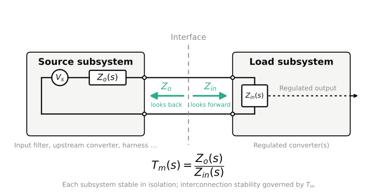
Middlebrook's Criterion in Practice: Input Filters, Cascaded Converters, and Distribution Buses
Middlebrook's criterion applied to the three interfaces where stable converters combine into unstable systems: input filters, cascaded stages, and distribution buses, each with a worked example and its fix.
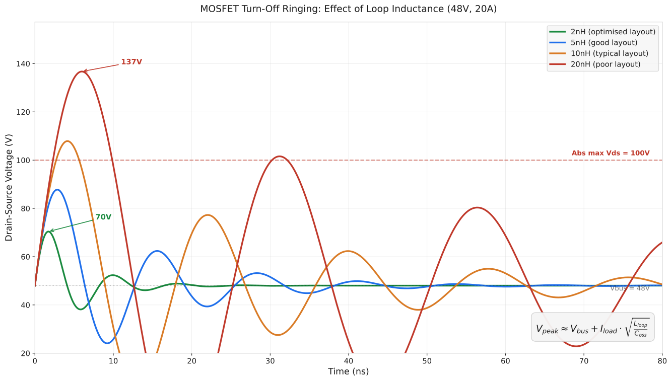
PCB Layout for Switchmode Converters: The Loops That Determine Whether Your Design Works
PCB layout for switching converters: find the critical high di/dt loops, minimise loop inductance, and avoid the mistakes that cause ringing and EMI.
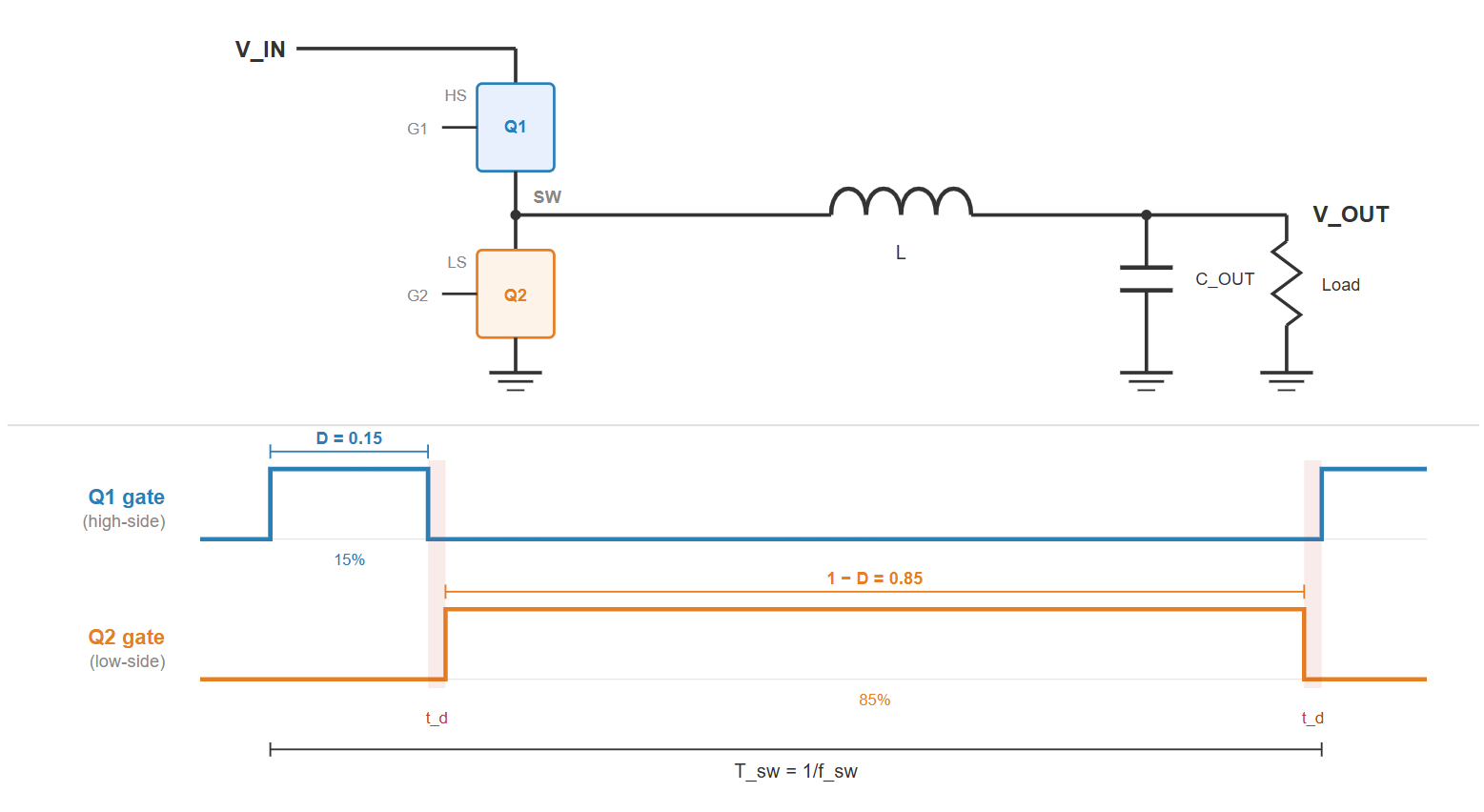
Why the Lowest RDS(on) Isn't the Best MOSFET for Your Buck Converter
How to choose a MOSFET for a buck converter: why the lowest RDS(on) loses on switching losses, with worked loss calculations for high and low side.
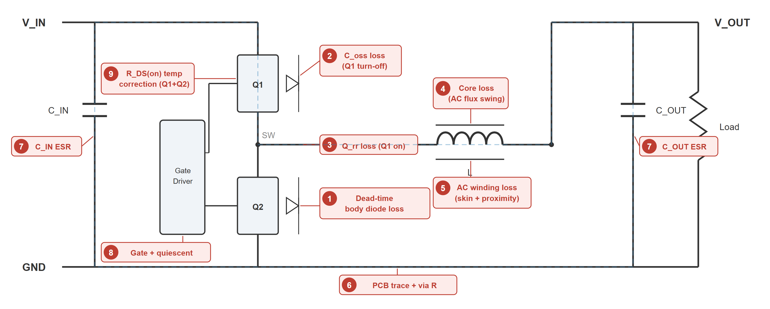
The Buck Converter Losses Nobody Tells You About
Nine buck converter loss mechanisms behind the gap between calculated and measured efficiency: dead time, body diode, gate drive and AC winding losses.
The Gap in Power Electronics Design Tools, and How We're Closing It
Why power supply design still relies on disconnected spreadsheets and SPICE, and how switchmode.io connects component selection, loss and stability analysis.