Why the Lowest RDS(on) Isn't the Best MOSFET for Your Buck Converter
How to choose a MOSFET for a buck converter: why the lowest RDS(on) loses on switching losses, with worked loss calculations for high and low side.
A practical walkthrough of MOSFET selection for a 12V-to-1.8V, 20A synchronous buck at 500kHz.
Sort the parametric search by , pick the lowest number that fits your package, move on to the inductor. I've done it. You've probably done it. It feels like the right approach because conduction loss is , and lower resistance means less loss. Except at 500kHz with a 12V input, the MOSFET with half the on-resistance can actually dissipate twice the power in the high-side position. The datasheet won't warn you about this because the parameters that cause it don't appear on the front page.
This article walks through how I'd select MOSFETs for a specific converter, starting from the constraints that eliminate most candidates before any loss calculation, then working through why the high-side and low-side positions need different parts, and finishing with a worked comparison using real numbers.
The design: 12V to 1.8V, 20A at 500kHz
The example throughout this article is a point-of-load converter you'd find on a server board or FPGA supply. = 12V, = 1.8V, 20A maximum load, 500kHz switching frequency. The duty cycle is:
That 15% duty cycle matters. The high-side MOSFET is on for 15% of each cycle and the low-side is on for 85%. They live very different lives, and treating them as interchangeable is where most selection mistakes start.
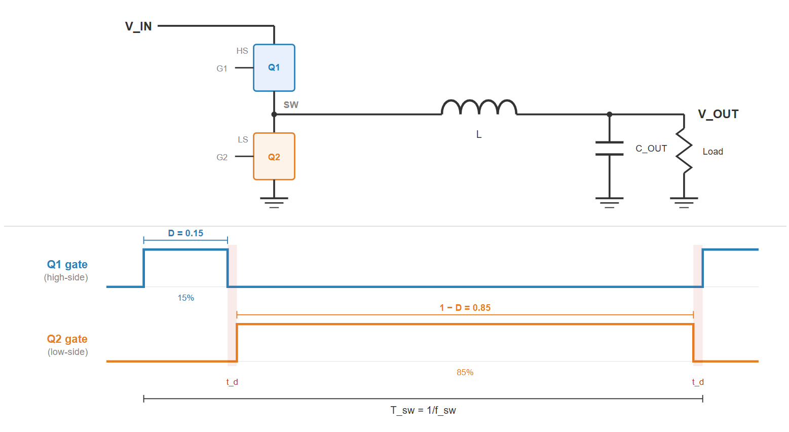
Fig. 1. Synchronous buck converter gate drive timing at D = 0.15. The high-side MOSFET conducts for 15% of each cycle, the low-side for 85%. The loss balance between the two positions is set by this ratio.
Constraints that eliminate 90% of candidates
Before opening a single datasheet, four constraints cut the field from hundreds of parts to maybe a dozen.
Voltage rating. The input is 12V, but voltage spikes from parasitic inductance in the power loop can easily reach 18-20V during switching transitions. A 25V MOSFET gives roughly 40% margin. A 30V part gives more headroom and is fine if the is competitive. Going to 60V or 100V is a common mistake for 12V applications: the higher voltage rating means a thicker drift region, which means higher per unit die area, higher , and higher . You pay for voltage headroom you don't need with worse performance in every parameter that matters.
For this design I'd look at 25V and 30V parts exclusively.
Package thermal limits. The SOA chart in the datasheet assumes a case temperature that depends on the test conditions. On a real board with no heatsink and a standard 4-layer PCB, a PowerPAK SO-8 might handle 2-3W before the junction temperature becomes a problem. A 5mm × 6mm TOLL package might manage 5-6W. This sets an upper bound on total MOSFET loss per device that no amount of low can fix. You could easily pick a 0.8mΩ part in a 3mm × 3mm DFN that could handle 40A on paper but couldn't dissipate the heat on an actual board at 20A.
Gate drive voltage. The controller or gate driver determines what the MOSFETs see. If you're using a 5V gate drive, you need logic-level MOSFETs specified at = 4.5V. The value at 4.5V is always higher than the headline number at 10V, sometimes by 30-50%. Check the correct column in the datasheet.
Availability. The MOSFET with the best parametrics is useless if it's on a 26 weeks lead time. For production designs, I check stock levels on at least two distributors and look for pin-compatible alternatives from a different manufacturer before committing. This isn't an exciting constraint, but it's the one that actually delays projects.
High-side and low-side are different jobs
In a synchronous buck, both MOSFETs carry the same average current, but the loss mechanisms are different for each position (Fig. 2).
The high-side MOSFET turns on with across it and the full load current flowing. Every turn-on and turn-off transition has a period where voltage and current overlap, dissipating power as crossover loss. It also charges and discharges every cycle, and at turn-on it has to supply the reverse recovery charge of the low-side body diode. These switching losses are proportional to , , and . At 500kHz with 12V and 20A, they add up quickly.
The conduction loss in the high-side is relatively small because it's only on for 15% of the cycle.
The low-side MOSFET is the opposite. It's on for 85% of the cycle, so conduction loss () dominates. Its switching losses are much lower because it turns on at near-zero (the body diode clamps the voltage during dead-time, then the channel takes over). The low-side doesn't see crossover loss at turn-on in the same way the high-side does.
But the low-side body diode matters. Its gets dumped through the high-side MOSFET at every turn-on transition. A low-side part with high penalises the high-side losses, not its own. This is an easy one to miss because the loss shows up in the wrong device.
The upshot: for the high-side, you want low , low , and fast switching, even if is moderate. For the low-side, you want the lowest you can get in a thermally capable package, with low .
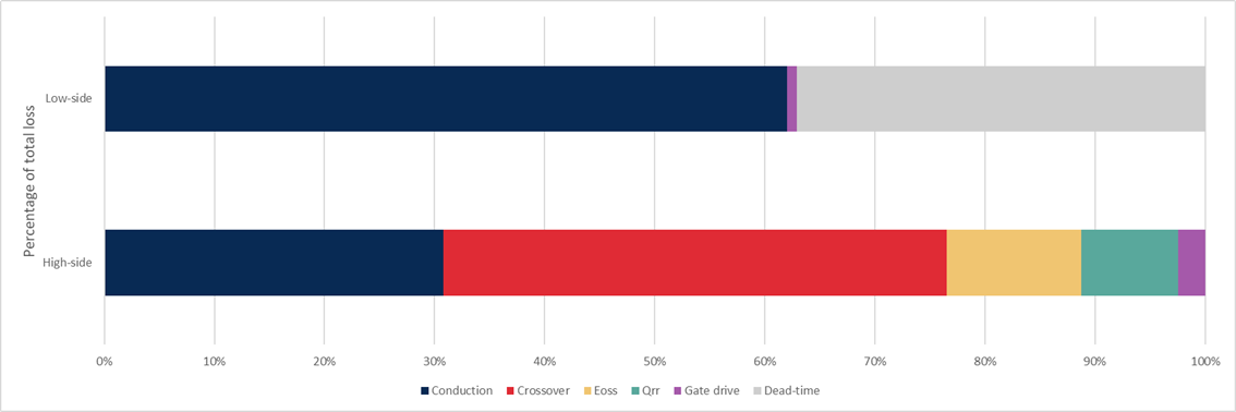
Fig. 2. Loss breakdown comparison for high-side vs. low-side at D = 0.15, 500kHz. Switching losses dominate the high-side, conduction loss dominates the low-side. Different loss profiles need different MOSFETs.
The trade-off in practice
The standard figure of merit (FOM) for power MOSFETs is . Lower is better. The logic is simple: sets conduction loss, sets switching loss, and minimising their product minimises total loss.
It's a useful first filter but it falls apart in practice for two reasons.
First, isn't what determines switching speed. (the gate-drain charge, or Miller charge) is what controls how fast transitions during turn-on and turn-off. Two MOSFETs with identical can have very different values, and the one with lower will switch faster and lose less energy per transition. Some manufacturers have optimised total by reducing (gate-source charge) while leaving untouched, which improves the FOM number without improving switching performance.
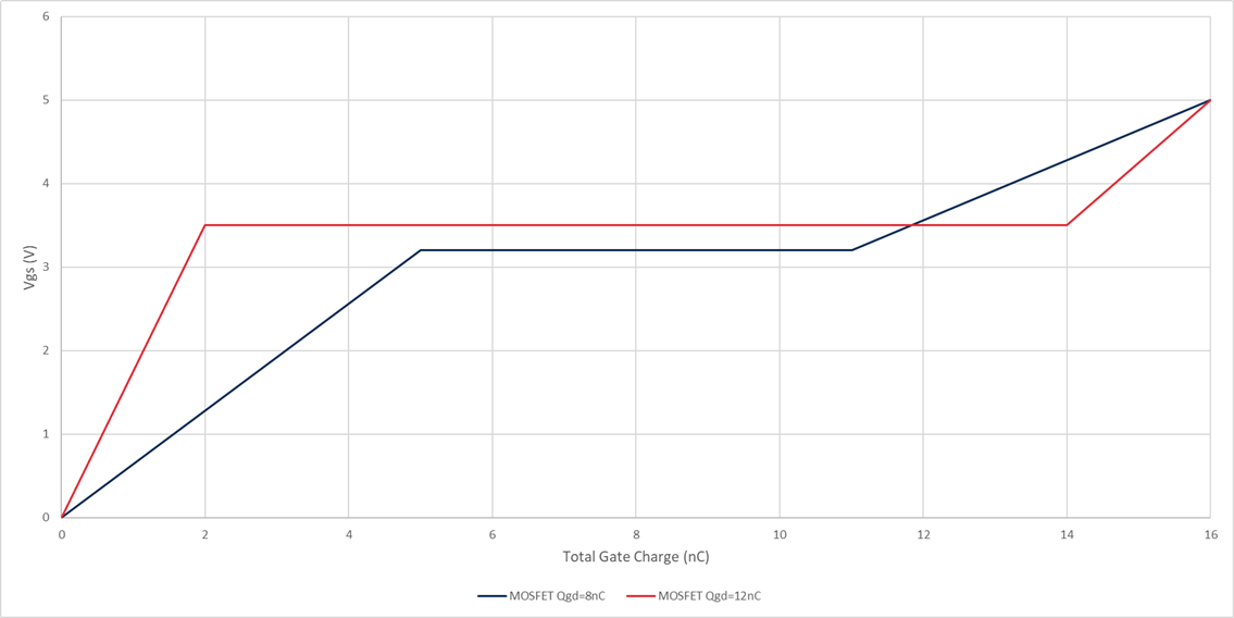
Fig. 3. Gate charge curves for two MOSFETs. One MOSFET has a short Miller plateau ( = 5nC) while another MOSFET has a long one ( = 12nC). The transition happens during the plateau, so sets switching speed, not total .
Second, the FOM treats high-side and low-side as the same job. They're not. Minimising gives you a compromise part that's acceptable in both positions but optimal in neither. At = 0.15, the high-side conduction loss is so small that trading higher for lower is almost always worth it. The FOM won't tell you that.
Let me put numbers on this. Take two hypothetical 30V MOSFETs in the same package:
MOSFET A (switching-optimised): = 4.5mΩ, = 12nC, = 3.5nC, = 0.3µJ, = 10nC. FOM = 54 mΩ·nC.
MOSFET B (conduction-optimised): = 1.8mΩ, = 45nC, = 12nC, = 0.8µJ, = 25nC. FOM = 81 mΩ·nC.
The FOM says MOSFET A is the better part. But better where?
The parameters the datasheet doesn't make obvious
Before running the loss comparison, a few of these numbers need adjusting from their datasheet values.
is quoted at 25°C. At a realistic junction temperature of 100°C, it increases by 40-50% for silicon MOSFETs. MOSFET A goes from 4.5mΩ to roughly 6.3mΩ. MOSFET B goes from 1.8mΩ to about 2.5mΩ. Use the hot numbers, not the headline.
is quoted at 25°C and at a specific di/dt and forward current. At 100°C junction, it can double. The 10nC and 25nC above might be 18nC and 45nC in a running converter. If your loss model uses room-temperature , you're underestimating the high-side turn-on loss.
is the energy stored in at a given voltage, and it's the right metric for switching loss (not , because is nonlinear). Not all datasheets provide directly. If yours gives a vs curve but no graph, you need to integrate it. I covered this in detail in a previous article - The Buck Converter Losses Nobody Tells You About.
sometimes needs extracting from the gate charge curve rather than reading a single number. The value at your operating (12V in this case) is what matters, not the value at whatever voltage the manufacturer chose for the test condition.
Worked selection: MOSFET A vs MOSFET B
Using the hot values, and the operating conditions of our 12V-to-1.8V, 20A, 500kHz converter.
High-side losses (D = 0.15):
The crossover transition time is set by and the effective gate drive current during the Miller plateau. The peak driver current might be 2A, but external gate resistance, internal , and driver output impedance reduce it. An effective 0.75A is realistic for most designs, giving .
| Loss mechanism | MOSFET A | MOSFET B |
|---|---|---|
| Conduction: | 20² × 6.3mΩ × 0.15 = 0.38W | 20² × 2.5mΩ × 0.15 = 0.15W |
| Crossover: | 0.5 × 12 × 20 × 9.3ns × 500kHz = 0.56W | 0.5 × 12 × 20 × 32ns × 500kHz = 1.92W |
| : | 0.3µJ × 500kHz = 0.15W | 0.8µJ × 500kHz = 0.40W |
| (low-side diode): | 18nC × 12 × 500kHz = 0.11W | 45nC × 12 × 500kHz = 0.27W |
| Gate drive: | 12nC × 5 × 500kHz = 0.03W | 45nC × 5 × 500kHz = 0.11W |
| Total high-side | 1.23W | 2.85W |
MOSFET B has 2.5× lower and saves 0.23W on conduction. But it loses 1.36W on crossover, 0.25W on , and 0.16W on . The net result is over twice the total loss in the high-side position. The part that looks better on the front page of the datasheet is the worse choice.
Low-side losses (1 - D = 0.85):
| Loss mechanism | MOSFET A | MOSFET B |
|---|---|---|
| Conduction: | 20² × 6.3mΩ × 0.85 = 2.14W | 20² × 2.5mΩ × 0.85 = 0.85W |
| Dead-time body diode: | 0.8 × 20 × 80ns × 2 × 500kHz = 1.28W | 0.8 × 20 × 80ns × 2 × 500kHz = 1.28W |
| Gate drive: | 12nC × 5 × 500kHz = 0.03W | 45nC × 5 × 500kHz = 0.11W |
| Total low-side | 3.45W | 2.24W |
Here MOSFET B wins by 1.2W, almost entirely from conduction loss. The dead-time loss is identical because it depends on the body diode forward voltage, not . Gate drive is negligible either way.
The optimal pairing: MOSFET A on the high side (1.39W — slightly higher than the above calculation due to using MOSFET B's ) and MOSFET B on the low side (2.24W) gives 3.63W total MOSFET loss. Fig. 4 shows the full loss breakdown side by side.
The lazy approach: MOSFET B in both positions (because it has the lowest ) gives 2.85 + 2.24 = 5.09W. That's 1.46W more, which at 36W output power is a 4% efficiency hit. Entirely avoidable.
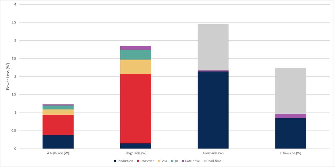
Fig. 4. Loss breakdown for MOSFET A and B in each position. MOSFET A wins the high side by over 2:1 on switching losses. MOSFET B wins the low side on conduction. The optimised pair (A high, B low) saves 1.46W over using MOSFET B in both positions.
When to use the same MOSFET for both
Using different parts for high-side and low-side adds BOM complexity, potentially complicates sourcing, and means two different gate drive characteristics to account for in your dead-time settings. Sometimes the gain isn't worth the hassle.
The optimisation matters most when is low (high step-down ratio, so the duty cycle mismatch between high and low side is large) and is high (so switching losses are a larger fraction of total loss). Our 12V-to-1.8V example at 500kHz is close to a worst case for using the same part.
If you're running a 12V-to-5V converter ( = 0.42) at 200kHz, the balance shifts. Both MOSFETs conduct for a more similar fraction of the cycle, and switching losses are 2.5× lower. The penalty for using a single part drops to maybe 0.5%, which most designs can absorb.
As a rule of thumb: if < 0.25 and > 300kHz, different parts are worth evaluating. Otherwise, a single part with a middle-ground FOM is usually fine.
GaN vs silicon: when does it make sense?
GaN FETs eliminate several of the problems above. Zero reverse recovery charge (no body diode in the traditional sense). Much lower and for a given . The EPC2045, for example, offers 5.6mΩ at 5V with just 6nC of total gate charge and negligible .
For our 12V, 20A, 500kHz example, a pair of EPC2045s would see roughly:
High-side total: 0.59W (conduction 0.44W, crossover 0.12W due to 0.8nC , negligible and no from the low-side). Low-side total: 2.83W (conduction 2.48W, dead-time 0.34W with 10ns dead-time instead of 80ns). Combined: 3.42W vs 3.63W for the optimised silicon pair, a saving of 0.21W.
But GaN comes with costs beyond the unit price.
Gate drive. The EPC2045 has a maximum of 6V. The recommended drive voltage is 5V with tight tolerance. There's no threshold voltage margin. You can't drive it from a standard 12V half-bridge driver with a bootstrap. You need a dedicated GaN gate driver with accurate voltage regulation on the gate supply. On a silicon design, 500mV of gate drive overshoot is absorbed by the 20V rating. On GaN, it kills the device.
No avalanche rating. Silicon MOSFETs can absorb energy during voltage spikes through avalanche breakdown. GaN FETs can't. Every voltage spike from layout inductance, load transients, or ringing that exceeds is potentially destructive. This means the PCB layout has to be much tighter, the input decoupling has to be closer, and you have less margin for error.
Thermal management. The EPC2045 is a 2.0mm × 1.5mm chip-scale package with no exposed pad or leads. All the heat exits through the solder bumps into the PCB. At 2W total it's manageable. At higher power levels or in constrained airflow, the thermal path becomes the limiting factor well before the FET's electrical limits.
Where the crossover sits. At 500kHz, the silicon pair is competitive enough that GaN's added design complexity might not justify the 0.21W saving, depending on how tight the thermal budget is. At 1MHz or above, the silicon switching losses roughly double while GaN's barely change, and the case for GaN becomes much stronger. Below 300kHz, silicon wins on cost, simplicity and possibly efficiency too.
I'd use GaN for this application if the switching frequency were above 1MHz or if the thermal constraints were very tight (fanless, small board area, high ambient). At 500kHz with reasonable cooling, optimised silicon is good enough and much simpler to design around. Fig. 5 shows where the crossover sits for this specific converter.
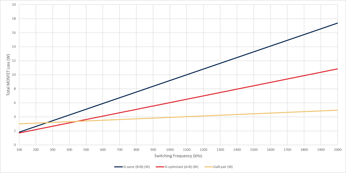
Fig. 5. Total MOSFET loss vs. switching frequency for the three configurations at 12V, 20A. Silicon losses scale with frequency due to crossover and . GaN stays nearly flat. The Si-to-GaN crossover sits around 450kHz for this application.
Quick reference
Table 1. MOSFET selection priorities by position in a synchronous buck converter.
| Parameter | High-side priority | Low-side priority | GaN advantage |
|---|---|---|---|
| Moderate (low reduces impact) | High (dominates loss) | Similar to best Si | |
| High (sets crossover loss) | Low (near-ZVS turn-on) | 5-10× lower than Si | |
| (total) | Moderate (gate drive loss) | Low | 5-10× lower |
| High (lost every cycle) | Low (often recovered via ZVS) | Much lower | |
| Low (but the low-side affects high-side loss) | High (lower is better for system) | Zero | |
| Thermal | Package must handle switching loss | Package must handle conduction loss | Limited by chip-scale package |
Table 2. When to use different high-side / low-side MOSFETs vs. the same part.
| Condition | Use different parts | Use same part |
|---|---|---|
| < 0.25 and > 300kHz | Yes, the gain is 2-4% efficiency | |
| > 0.35 or < 300kHz | Yes, the gain is < 1% | |
| BOM cost is critical | Yes, volume pricing on one part | |
| Second-sourcing is difficult | Yes, fewer qualifications needed |
The MOSFET selection process has a tendency to get treated as a lookup table exercise. Sort by , check the voltage rating, done. For low-frequency designs with moderate step-down ratios, that's often good enough. But for the converters where efficiency actually matters, at high frequency and high step-down, spending an hour on the loss comparison between two or three candidates is time well spent. The difference between the lazy pick and the optimised pair was 4% in this example. On a 200W converter, that's 8W of heat you don't need to deal with.