The Buck Converter Losses Nobody Tells You About
Nine buck converter loss mechanisms behind the gap between calculated and measured efficiency: dead time, body diode, gate drive and AC winding losses.
Why your efficiency calculator says 95% but your bench measurement says 89%.
Your MOSFET conduction and switching losses are already in the spreadsheet. This article is about everything else — the collection of second-order loss mechanisms that individually look negligible on paper but collectively account for that gap between calculated and measured efficiency. I've spent enough time staring at thermal images of boards that should have been cooler to know these add up faster than you'd expect. Fig. 1 shows where each one lives in the circuit.
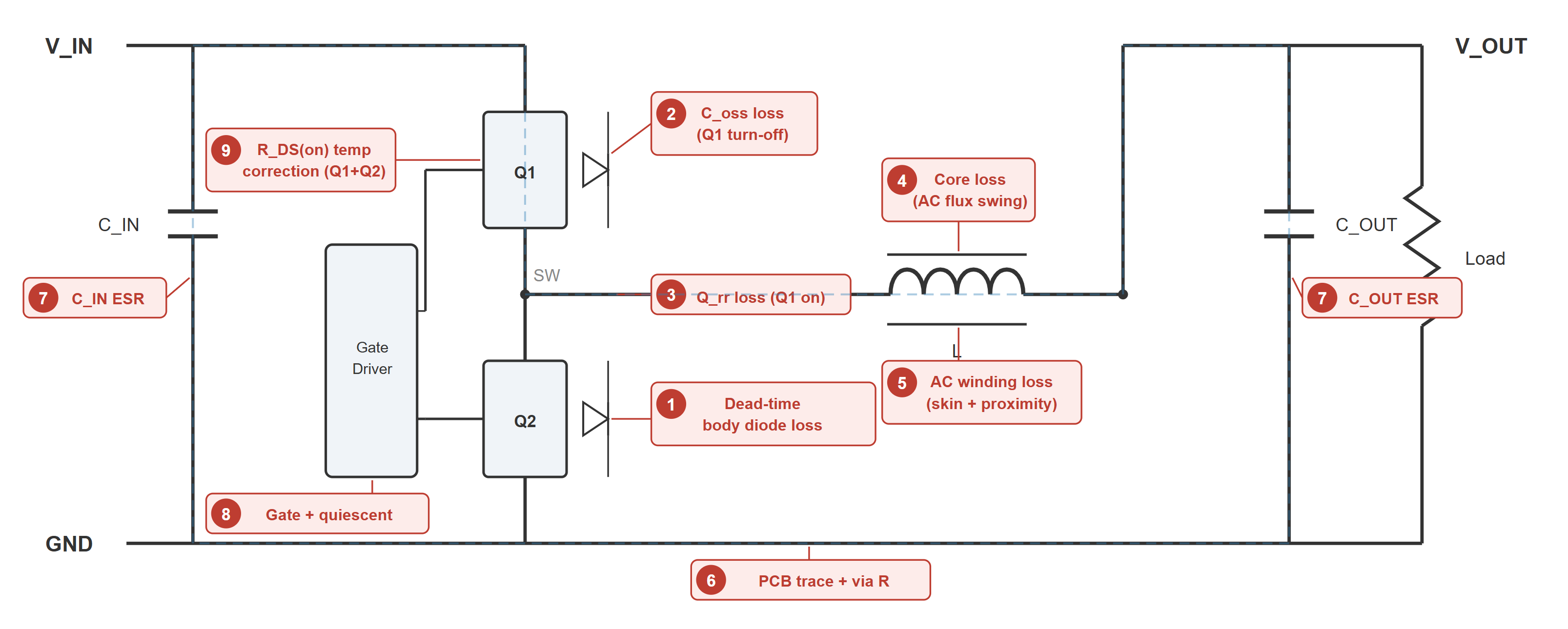
Fig. 1. Synchronous buck converter with the nine loss mechanisms covered in this article marked at their physical locations.
Dead-time body diode conduction
On a 48V-to-12V converter I was working on last year, the efficiency was about 2% below what my loss model predicted at full load. The MOSFET selection was solid, the inductor DCR was low, and the PCB layout was tight. The culprit turned out to be dead-time — 100ns of it, which I hadn't questioned because it was the controller's default.
In a synchronous buck, there's a brief interval during every switching cycle where neither MOSFET is on [2] (Fig. 2). The inductor current still flows, and it forces its way through the low-side MOSFET's body diode. That body diode has a forward drop of 0.7–1.2V, compared to the millivolts you'd see across the channel during normal conduction.
At 20A load current, a 4mΩ device dissipates 1.6W instantaneously through . During dead-time, that same 20A through a 1.0V body diode dissipates 20W instantaneously, over 12× more loss per unit time. At 500kHz with 80ns total dead-time per cycle, the body diode conducts for 4% of each period giving an of 0.8W, certainly not an insignificant amount.
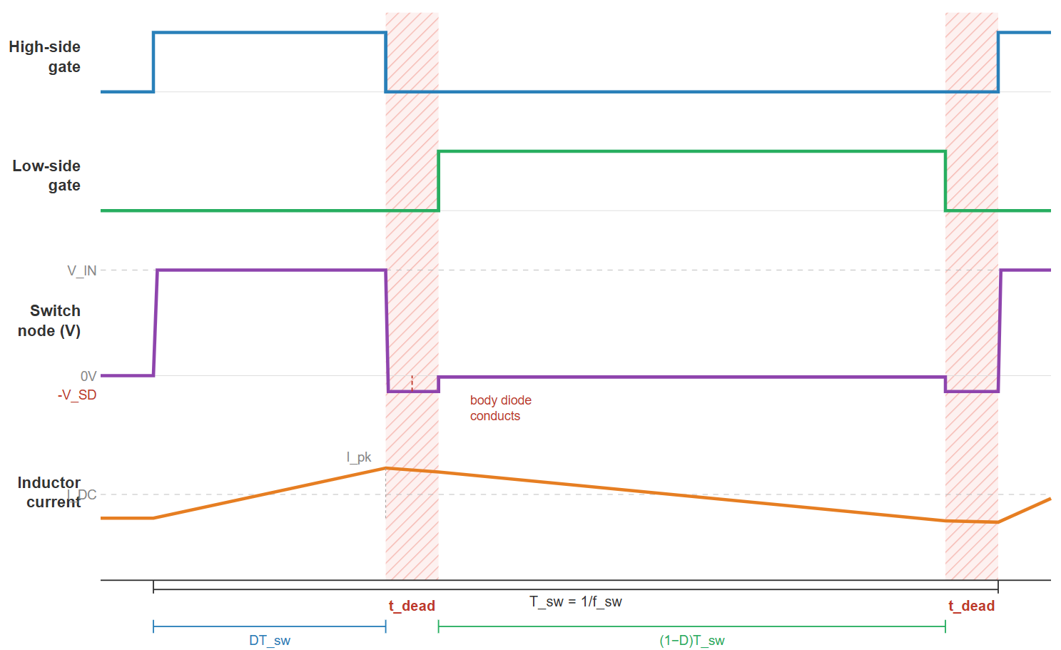
Fig. 2. Single switching cycle showing the dead-time intervals where body diode conduction occurs. The shaded regions represent the periods where neither MOSFET is on and the inductor current flows through the low-side body diode at .
The loss is simple to estimate:
Where is the body diode forward voltage and / are the dead-times at each transition edge.
Most controllers set dead-time conservatively. They'd rather waste efficiency than risk shoot-through [1]. Some offer adaptive dead-time that minimises the window automatically. If you're using a controller with fixed dead-time at high currents, check what it's actually set to. On that 48V design, switching to a controller with adaptive dead-time recovered about 1.5% efficiency at full load.
MOSFET output capacitance () losses
Every MOSFET has parasitic capacitance between drain and source () and between gate and drain (). Together these form . Each switching cycle, the high-side MOSFET's charges from 0V to when it turns off, and that stored energy is lost.
The textbook equation is:
The trouble with this equation is that varies with applied voltage by a factor of 3–10× across the operating range [2], [3], as Fig. 3 illustrates. The datasheet value at 100V tells you almost nothing about behaviour at 5V or 300V. A MOSFET with 76pF of at 100V might have 4nF at 5V and 37pF at 300V. Plugging any single value into gives you a number, but not necessarily the right one.
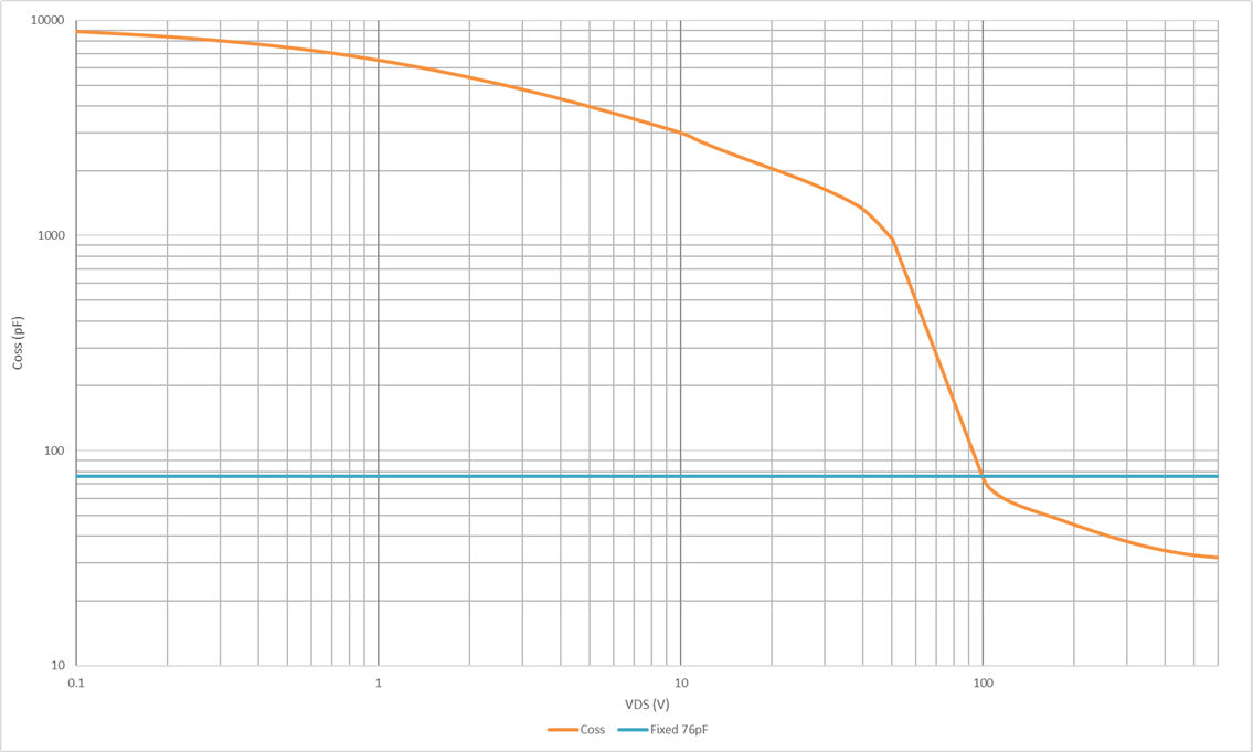
Fig. 3. vs. for a STB24N60M6 MOSFET compared with the fixed 76pF datasheet value. The nonlinearity means a single-value calculation can be off by 3-10×.
What you actually want is , the energy stored in when charged to your input voltage [3]. Better datasheets provide this as a graph of vs. . If yours doesn't, you need to integrate the curve, or use the manufacturer's simulation models. The power loss then becomes:
I've found that the simple calculation using the 100V datasheet value can be off by a substantial amount compared to the integrated , as Fig. 4 illustrates.
For example, a STB24N60M6 MOSFET might store 0.3µJ in at 50V. At 500kHz, that's 0.15W. Scale to 600V input and the loss goes up by 16× to 5W due to the term, which is why loss often dominates in higher-voltage applications.
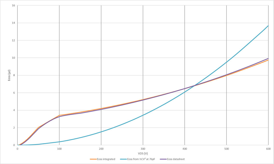
Fig. 4. datasheet vs. for a STB24N60M6 MOSFET compared with the from integrated and from at 76pF.
One thing that took me a while to appreciate is that the low-side MOSFET's loss is often recoverable [4]. If there's enough inductor current at the transition point, it discharges before turn-on, giving you partial or full zero-voltage switching (ZVS). At heavy load this usually works. At light load there isn't enough energy in the inductor, and loss comes back. That's one reason efficiency curves sag at low current.
Reverse recovery charge ()
This ties back to dead-time. When the low-side body diode is conducting and the high-side MOSFET turns on, the diode doesn't stop conducting instantly. Stored charge carriers in the junction take time to sweep out, and during that process a pulse of current flows backwards through the diode and straight through the high-side MOSFET from to ground.
This reverse recovery current creates loss in two ways. First, the high-side MOSFET has to handle the extra current during turn-on, increasing switching loss. Second, the recovered charge energy () is dissipated directly as heat.
For our test case STB24N60M6 MOSFET, has a value of 2.3μC, this gives a loss of 69W at 60V, 500kHz, clearly this is not a suitable MOSFET for this application and shows how it can take just one value to be a showstopper, and perhaps not the value you expect. What makes this tricky to account for is the temperature dependence: can increase by 2–3× between 25°C and 125°C junction temperature [5], [6]. This creates a feedback loop where more loss raises the temperature, which increases , which increases loss. It does converge, hopefully, but to a worse operating point than you'd calculate from the 25°C datasheet values.
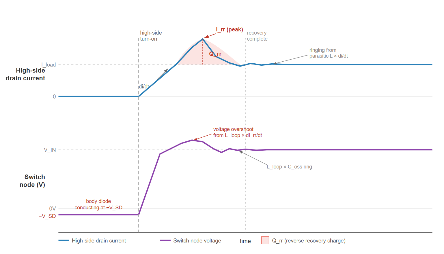
Fig. 5. Switch node voltage and high-side drain current at turn-on, showing the reverse recovery current spike. The shaded area under the spike equals .
When choosing between two otherwise similar MOSFETs, lower wins in a hard-switched buck. Some manufacturers now offer devices with integrated Schottky diodes that conduct preferentially during dead-time, preventing the body diode from storing charge in the first place.
Inductor core losses
I'll admit this is the one that caught me out most when I first started doing power design. DCR is on the front page of every inductor datasheet, the calculation is simple, and it's easy to assume that's the whole story. It isn't.
The loss comes from the AC flux swing in the core, driven by inductor ripple current. It's the ripple that matters, not the DC component (DC contributes to saturation, not core loss). The Steinmetz equation [7] gives a rough estimate based on material, frequency, flux swing, and core volume:
Where , , and are material constants that most off-the-shelf inductor datasheets don't provide. And the core materials in commodity inductors, especially cheaper ferrite bobbins, often have higher losses than you'd expect from the limited data given. I've seen forum posts from engineers consistently reporting the same thing, measured inductor temperatures higher than DCR losses alone can explain, especially above 50kHz.
There's a subtlety here that's easy to miss. If you keep the same inductor and increase switching frequency, ripple current drops as and core loss can actually decrease. That looks like a free win, but it never happens in practice. When you push frequency up, you reduce inductance to shrink the part. The ripple stays roughly the same or gets worse. Fig. 6 shows the realistic case: the inductor is redesigned at each frequency to maintain a constant ripple ratio, and core loss scales as , overtaking DCR loss around 150–200kHz.
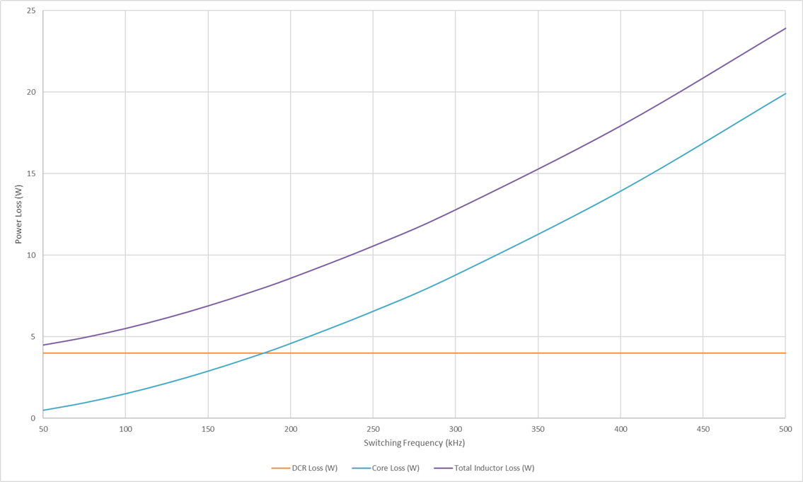
Fig. 6. DCR loss (flat) vs. core loss (rising) across switching frequency, assuming the inductor is redesigned at each frequency to maintain constant ripple ratio. Core loss overtakes DCR around 150–200kHz and reaches 5× DCR by 500kHz.
Core loss scales roughly with to depending on material, so doubling your switching frequency can increase core loss by 3–6×. You can reduce it by increasing inductance (less ripple current means less AC flux swing), but that usually means accepting higher DCR. It's a genuine trade-off, and the crossover point depends on your operating frequency and load current. If your inductor is warmer than DCR losses predict, core loss is almost certainly why. Powdered iron cores tend to be the worst offenders at high frequency, despite their better DC bias performance compared to ferrite.
Coilcraft and Würth both provide online loss calculators for their specific parts that account for core material properly [8].
AC winding losses: skin and proximity effects
Even the copper resistance isn't as simple as the DC value. At switching frequencies, two electromagnetic effects push the effective winding resistance above DCR [9].
Skin effect concentrates current towards the outer surface of the conductor, reducing the effective cross-section. The skin depth in copper at 500kHz is about 93µm. If your inductor uses wire thicker than roughly twice that diameter, the centre of the wire carries very little current at the switching frequency.
Proximity effect is often worse. Current in adjacent turns creates magnetic fields that force current in neighbouring conductors to crowd to one side. In multi-layer windings, proximity effect alone can push the AC resistance to 5–10× the DC value [10].
The ratio is what matters. Only the ripple current sees this higher resistance, not the DC component, so the impact depends on your ripple fraction. But in designs where I've pushed switching frequency above 500kHz to shrink the inductor, this has added measurable loss that didn't appear in a DCR-only calculation.
The practical takeaway of this is that increasing switching frequency hits the inductor twice over, through higher core loss and higher AC winding loss. And if you reduce inductance to keep the part small, higher ripple current amplifies both.
The key parameter is the ratio of wire diameter to skin depth, . The skin depth in copper at 20°C is:
Which gives = 0.21mm at 100kHz, 0.13mm at 250kHz, 0.093mm at 500kHz, and 0.066mm at 1MHz.
Once you know for your wire gauge and switching frequency, the winding loss depends heavily on the number of layers. Table 1 shows values computed from Dowell's equation [9] for closely-packed round wire windings:
| 1 layer | 2 layers | 3 layers | 5 layers | |
|---|---|---|---|---|
| 0.5 | 1.0 | 1.0 | 1.1 | 1.2 |
| 1.0 | 1.1 | 1.4 | 1.9 | 3.6 |
| 1.5 | 1.4 | 2.8 | 5.1 | 13 |
| 2.0 | 1.9 | 5.1 | 11 | 28 |
| 3.0 | 3.0 | 9.5 | 20 | 55 |
Table 1. vs. normalised wire diameter and number of winding layers, computed from Dowell's equation [9].
The layer count effect is what catches people out. At = 1.5, a single-layer winding barely notices the AC effects ( ≈ 1.1), but a three-layer winding sees nearly 8× the DC resistance. Ridley [11] gives a worked example: five layers of 0.3mm wire at 100kHz ( ≈ 1.5) gives an average of 11.6, with the innermost layer reaching 27×. Doubling the wire to 0.6mm ( ≈ 3) makes it 51× average, with the inner layer at 123×. Thicker wire made the losses worse, not better.
PCB trace and via resistance
No component datasheet accounts for this one. It's entirely a function of your layout, and at high currents it can be significant.
A 1oz (35µm) copper trace that's 10mm long and 2mm wide has roughly 2.5mΩ of resistance. A buck converter's power loop might include 30–50mm of total trace length at various widths. Add in a few vias (each roughly 0.5–1mΩ for a 0.3mm via in 1oz copper) and you can easily accumulate 10–20mΩ of parasitic resistance in the power path.
At 10A, 10mΩ costs you 1W. At 20A, 4W. That won't appear in any simulation that doesn't model the PCB, and most don't.
I made this mistake on an early design where I was fixated on getting the MOSFET and inductor selection perfect, then routed the power path through a couple of vias and a narrow trace segment because it was the easiest way to get the layout to fit. The board ran 3°C hotter on one side than the other, and it took a thermal camera to figure out the trace between the inductor and the output caps was the issue. An embarrassingly simple fix — widening the trace and adding parallel vias — dropped the hot spot by 2°C and recovered about 0.3% efficiency. Not dramatic, but it was free.
Trace DC resistance is calculated from the bulk resistivity of copper ( = 1.72 × 10⁻⁸ Ω·m at 20°C):
Where is trace length, is width, and is copper thickness. Table 2 gives the resistance per centimetre of trace length for common widths in 1oz and 2oz copper.
| Trace width | 1oz (35µm) | 2oz (70µm) |
|---|---|---|
| 1mm | 4.9 mΩ/cm | 2.5 mΩ/cm |
| 2mm | 2.5 mΩ/cm | 1.2 mΩ/cm |
| 5mm | 1.0 mΩ/cm | 0.49 mΩ/cm |
| 10mm | 0.49 mΩ/cm | 0.25 mΩ/cm |
Table 2. PCB trace DC resistance per centimetre at 20°C, calculated from with = 1.72 × 10⁻⁸ Ω·m.
Note these are DC values at 20°C. Copper's temperature coefficient adds roughly 0.4% per degree, so a board running at 60°C sees about 15% higher trace resistance than the table values. For current-carrying capacity and thermal limits, IPC-2221 [12] provides empirically-derived derating curves.
Use 2oz copper on power layers where you can. Keep the high-current loop as short and wide as possible. Use multiple vias in parallel for any power path that changes layers. And don't forget the ground return; current flowing back through the ground plane sees resistance too.
Input and output capacitor ESR
The input capacitors in a buck converter live a hard life. The RMS ripple current through them is [13]:
This peaks at 50% duty cycle (Fig. 7), where the input cap RMS current equals half the load current. At 10A load and , that's 5A RMS through your input caps. With a single ceramic at 5mΩ ESR, the loss is 125mW. With an aluminium electrolytic at 50mΩ, it's 1.25W, and the cap will be warm to the touch.
Output cap ESR losses are usually smaller since the output only sees the inductor ripple current, but they're not zero with electrolytics.
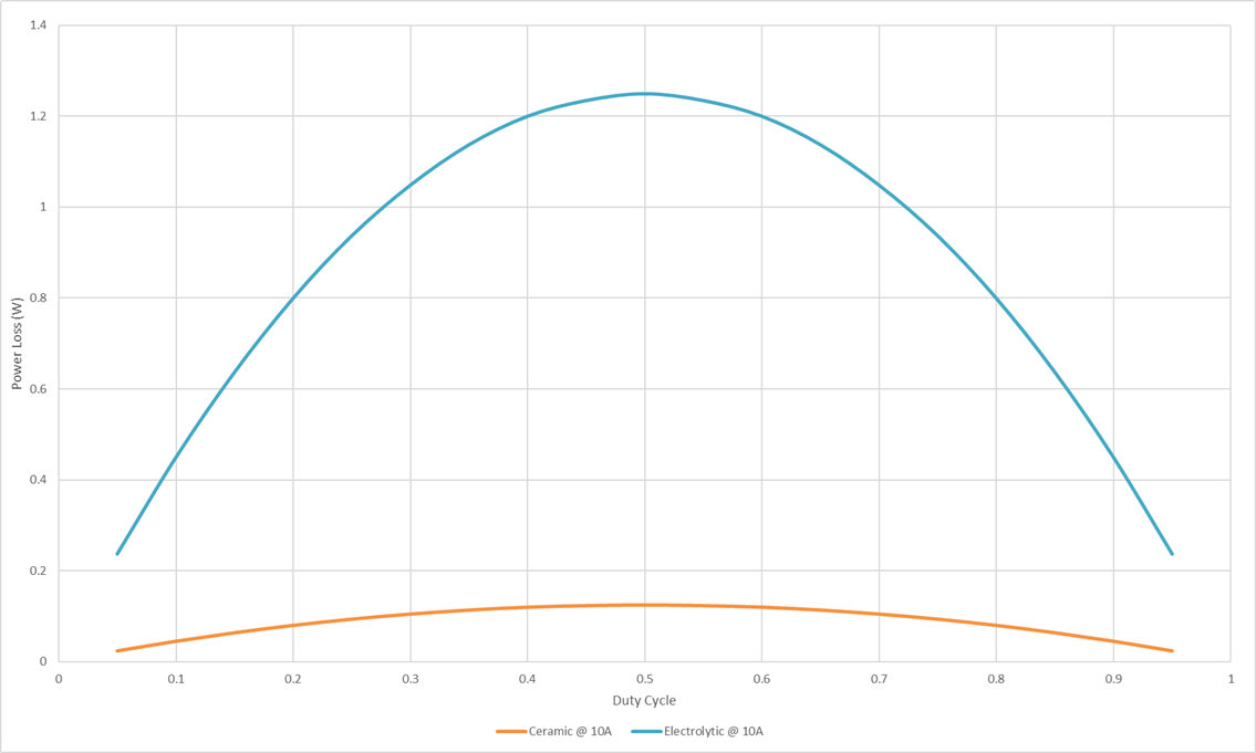
Fig. 7. Input capacitor power loss vs. duty cycle at 10A load current for a ceramic and electrolytic capacitor. The parabolic shape peaks at D = 0.5, where the input cap sees half the load current as RMS ripple.
There's a related trap with class 2 ceramic capacitors as effective capacitance drops with DC bias. A 10µF X5R ceramic rated for 25V might deliver only 4–5µF at 20V. With less actual capacitance, voltage ripple increases. Check the manufacturer's DC bias curves, they're usually available but buried in the small print.
Gate driver and quiescent losses
Light-load efficiency is where these losses bite hardest. I lost an afternoon once trying to work out why a low-power sensor node running off a 500mW supply was stuck at 87% efficiency. The power stage looked clean. Turned out the gate drive and controller quiescent draw were eating 65mW between them, which at that power level is 13% gone before the converter does anything useful.
Each switching cycle, the gate charge of both MOSFETs has to be supplied by the driver. The energy comes from and is dissipated in the driver and MOSFET gate resistance:
For a MOSFET with 20nC gate charge driven at 5V and 500kHz, that's 50mW per device, 100mW total. In a 50W converter, barely noticeable. In a 1W converter running the same switching frequency, that's 10% of your output power gone on gate drive alone.
The controller IC's quiescent current adds to this. Modern controllers draw 0.5–5mA depending on features and oscillator frequency. At 5V input with 5mA draw, that's 25mW of overhead regardless of load.
These are the losses that create the characteristic droop on the left side of every buck converter efficiency curve (Fig. 8). Everything else scales down with load current (most of it with I²), but gate drive and quiescent losses stay roughly constant. It's why pulse-skipping and burst modes exist, by reducing the effective switching frequency at light load, they cut gate drive losses roughly in proportion.
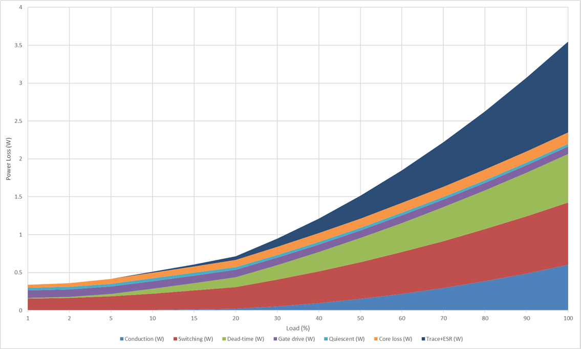
Fig. 8. Efficiency vs. load for a 12V-to-3.3V, 10A, 500kHz buck converter, with stacked loss breakdown showing the transition from gate drive/quiescent-dominated loss at light load to conduction-dominated loss at full load.
at actual junction temperature
This isn't a separate loss mechanism, it's a correction to the conduction loss you've already calculated, and it's almost always underestimated.
MOSFET datasheets quote at 25°C. Your MOSFET junction sits at 60–120°C in a real design. The temperature coefficient for silicon MOSFETs runs at about 0.4–0.7% per degree above 25°C. Take the STB24N60M6 as an example: 162mΩ at 25°C becomes 294mΩ at 100°C, a 55% increase. That's typical, not worst-case.
If your efficiency calculator used the 25°C value, your conduction losses are 1.3–1.5× what you think they are. Use the normalisation curve ( vs. temperature) from the datasheet, not the headline number. Fig. 9 shows how three different MOSFETs compared across the full temperature range.
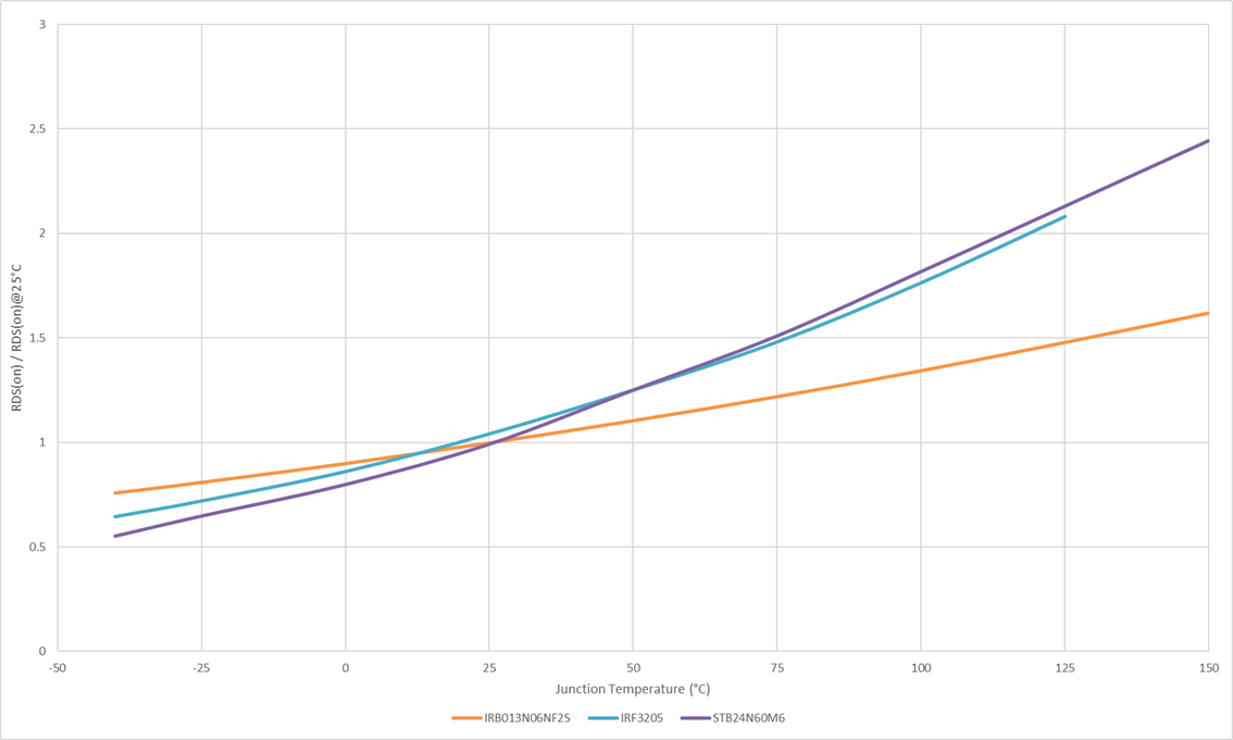
Fig. 9. normalised to 25°C value vs. junction temperature for three MOSFETs: IRB013N06NF2S, IRF3205, and STB24N60M6. All reach 1.5–2× by 125°C.
This also creates a thermal feedback effect: higher temperature → higher → more loss → higher temperature. It converges, hopefully, but always to a worse steady-state than a cold calculation would suggest.
Which of these matter for your design?
These losses don't all contribute equally. What dominates depends on where you're operating. Table 3 gives a quick reference for which mechanisms matter most under four common conditions.
If you're pushing switching frequency above 500kHz for a compact design, inductor core loss, AC winding loss, loss, and gate drive loss all scale with frequency. These are likely the biggest contributors to your efficiency gap. I'd start the investigation there.
At high output current above 10A, the -scaling losses take over: PCB trace resistance, capacitor ESR, dead-time conduction, and the temperature correction. These grow fast with current and are easy to underestimate because no single one looks large in isolation.
For high input voltage applications above 24V, focus on (scales with ) and (scales with ). A 48V design sees 16× the loss of a 12V design for the same MOSFET.
At light load, none of the above matters much. Gate drive and quiescent current dominate, and the fix is either a lower- MOSFET, a lower-quiescent controller, or a control scheme that reduces effective switching frequency at light load.
| Loss mechanism | High freq (>500kHz) | High current (>10A) | High (>24V) | Light load (<10%) |
|---|---|---|---|---|
| Dead-time body diode | Dominant | Dominant | Moderate | Negligible |
| Dominant | Negligible | Dominant | Moderate | |
| Dominant | Moderate | Dominant | Negligible | |
| Inductor core loss | Dominant | Moderate | Negligible | Negligible |
| AC winding loss | Dominant | Moderate | Negligible | Negligible |
| PCB trace resistance | Negligible | Dominant | Negligible | Negligible |
| Capacitor ESR | Negligible | Dominant | Negligible | Negligible |
| Gate drive / quiescent | Dominant | Negligible | Negligible | Dominant |
| temp correction | Negligible | Dominant | Negligible | Negligible |
Table 3. Relative significance of each loss mechanism across four common operating conditions.
The gap between calculated and measured efficiency is almost never one big mistake. It's the accumulation of many effects, each contributing a fraction of a percent, that together account for the difference. Knowing where to look for your specific application is more than half the battle.
If I could go back and change one thing about how I learned this, it would be building a loss budget spreadsheet that includes all nine mechanisms from the start, even when I thought they were negligible. The ones I left out of early designs were always the ones I spent the most time debugging later.
References
[1] Vishay Siliconix, "Optimum dead time selection in ZVS topologies," Application Note, 2012. [Online]. Available: https://www.vishay.com/docs/49932/49932.pdf
[2] EPC, "AN030: Hard switching losses calculations," Application Note, 2024. [Online]. Available: https://epc-co.com/epc/Portals/0/epc/documents/application-notes/AN030%20Hard%20Switching%20Losses%20Calculation.pdf
[3] Infineon, "CoolMOS detailed MOSFET behavioral analysis," Application Note, 2018. [Online]. Available: https://www.farnell.com/datasheets/2354900.pdf.
[4] Vishay Siliconix, "Beware of zero voltage switching," Application Note. [Online]. Available: https://www.mouser.com/pdfdocs/Vishay_Zero_Voltage_Switching.pdf
[5] S. Park et al., "Temperature-dependent reverse-recovery behavior analysis and circuit-level mitigation of superjunction MOSFETs," Micromachines, vol. 16, no. 11, p. 1252, Oct. 2025. [Online]. Available: https://www.mdpi.com/2072-666X/16/11/1252
[6] STMicroelectronics, "AN5028: Calculation of turn-off power losses generated by an ultrafast diode," Application Note, 2018. [Online]. Available: https://www.st.com/resource/en/application_note/an5028-calculation-of-turnoff-power-losses-generated-by-a-ultrafast-diode-stmicroelectronics.pdf
[7] Analog Devices, "Addressing core loss in coupled inductors," Application Note. [Online]. Available: https://www.analog.com/en/resources/app-notes/addressing-core-loss-in-coupled-inductors.html
[8] Würth Elektronik, "ANP029: Accurate inductor loss determination using REDEXPERT," Application Note, 2015. [Online]. Available: https://www.we-online.com/components/media/o109035v410%20AppNotes_ANP029_AccurateInductorLossDeterminationUsingRedExpert_EN.pdf
[9] S. Zurek, "Proximity effect," Encyclopedia Magnetica, 2024. [Online]. Available: https://www.e-magnetica.pl/doku.php/proximity_effect
[10] X. Nan and C. R. Sullivan, "An improved calculation of proximity-effect loss in high-frequency windings of round conductors," in Proc. IEEE Power Electron. Specialists Conf., 2003, pp. 853–860. [Online]. Available: https://www.wcmagnetics.com/wp-content/uploads/2015/02/proximityeffect.pdf
[11] R. Ridley, "Proximity loss," Switching Power Magazine, 2005. [Online]. Available: https://ridleyengineering.com/images/phocadownload/13%20proximity%20loss.pdf
[12] DigiKey, "PCB trace width calculator (IPC-2221)," Online Tool. [Online]. Available: https://www.digikey.com/en/resources/conversion-calculators/conversion-calculator-pcb-trace-width
[13] ROHM, "Efficiency of buck converter," Application Note 64AN035E, Rev. 004, Nov. 2022. [Online]. Available: https://fscdn.rohm.com/en/products/databook/applinote/ic/power/switching_regulator/buck_converter_efficiency_app-e.pdf