This is one synchronous buck, 12V to 3.3V at 10A, taken from specification to part numbers twice. The first build follows the simple estimate at every step. The second checks each part at the corner where it's weakest. Both come out at 95.2% efficient at 12V. The first one runs its inductor 10°C past the part's own temperature limit. Its input ripple is 2.6 times the estimate, and its output holds half the capacitance the load step needs.
None of those failures shows up in the efficiency figure. Each one is a datasheet number read at the wrong condition. I'll go through the steps in order, name the part the simple estimate picks, and show where it misses. Both builds use real parts, and I solved both through the analysis engine switchmode.io is being built on.
The specification
| Parameter | Value |
|---|---|
| Input | 12V ±10%, so 10.8V to 13.2V |
| Output | 3.3V at 10A |
| Switching frequency | 500kHz |
| Inductor ripple | 30% of the load current, at maximum input |
| Gate-driver supply | 5V |
| Ambient | 50°C |
At 10A a discrete pair of MOSFETs is still the usual choice. At 5A most designers would pick a buck IC with its switches inside, and the MOSFET step below wouldn't apply. The ambient is inside an enclosure, and it matters more than any other line in that table.
Step 1: the duty cycle at each end of the input range
The simple estimate takes the duty cycle at 12V and moves on:
where is the duty cycle, is the 3.3V output and is the input voltage. This is the lossless form. The losses add a little at full load.
At 12V, = 0.275. Across the range it runs from 0.306 at 10.8V to 0.250 at 13.2V.
That spread is small, but it decides where every later check has to be made. The inductor ripple is largest at 13.2V. The input capacitors' RMS current is largest at 10.8V. And the capacitance the input capacitors keep is smallest at 13.2V. A design checked at 12V alone is checked at a corner where none of those is worst.
Step 2: inductance
The inductor ripple current is
where:
- is the peak-to-peak inductor ripple current, in amps
- and are the input and output voltages, and is the duty cycle from step 1
- is the switching frequency, 500kHz
- is the inductance, in henries
For 30% ripple at 13.2V, that's 1.65µH. I took 1.5µH, the nearest standard value. It gives 3.06A of ripple at 10.8V and 3.30A at 13.2V, so the worst case is at maximum input. The buck inductor calculator does this step and the CCM/DCM boundary across the whole input range.
The two currents the inductor has to carry follow from that:
where is the peak inductor current, the RMS inductor current, the 10A load and the ripple current from above. At 13.2V they're 11.65A and 10.05A.
This step is where the simple estimate is closest to right. The trouble starts when those two numbers go to a datasheet.
Step 3: the inductor's ratings
The simple estimate checks one rating: saturation current above the peak. Wevolver's worked example of the same conversion, at 5A, says "Select an inductor rated above 6 A saturation current" [1]. On that test, Murata's 1274AS-H-1R5N passes easily. Its guaranteed saturation current is 15.3A, defined as a 30% drop in inductance, which is 1.31 times the 11.65A peak [2].
The rating that decides this design is the other one. Murata defines the temperature-rise current as the DC current that raises the part 40°C "on our PCB for test purpose" [3]. For this part that's 10.5A typical and 8.9A guaranteed [2]. The RMS current is 10.05A. Read the typical column and there's 4% margin. Read the guaranteed one and the design is already 13% over.
The temperature limit settles it. Murata gives the operating range as −40°C to +85°C and says it includes "self temperature rise" [3]. So the part's own heating counts against the 85°C. At 50°C ambient, the inductor can afford a 35°C rise.
The first rise I worked out was 36°C, read off Murata's DC temperature-rise curve at 10.05A. That looked like a 1°C miss, close enough to argue about. It leaves out the ripple. The solve adds the AC winding and core loss from the part's measured AC resistance, 0.11W on top of 0.75W in the DC resistance. With that, the part reaches 95.0°C at 13.2V, a 45°C rise.
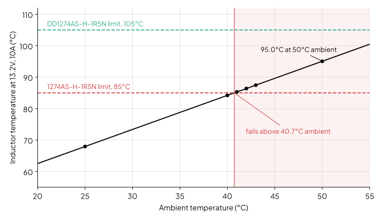
Fig. 1 shows the same solve across ambient temperatures. The part passes up to about 40.7°C and fails above it. A design checked at 25°C on the bench would pass with 17°C to spare.
The fix in the same footprint is the DD1274AS-H-1R5N. It has the same inductance, DC resistance and current ratings, and Murata rates it to 105°C, again including self-heating [4]. It reaches 95.1°C, 10°C inside its limit. That margin assumes the typical DC resistance, 6.4mΩ. At Murata's maximum of 7.7mΩ, the DC loss rises by a fifth and I estimate the part at about 103°C. That's a pass by 2°C, which I'd want to check on the board.
A larger part fixes it properly. Coilcraft's XAL1010-152MED is 1.5µH with 1.6mΩ typical resistance and a 40.5A rating for a 40°C rise [5]. It weighs about three times as much, so it isn't a drop-in swap. The inductor sizing article covers the ripple-ratio choice that sits behind all of this.
Step 4: input capacitors
The input capacitors supply the pulsed current the high-side switch draws. The ripple across them is
where:
- is the peak-to-peak input ripple voltage
- is the 10A load and the duty cycle from step 1
- is the 500kHz switching frequency
- is the input capacitance, in farads
The simple estimate puts the marked value in for . Wevolver suggests "two to three 10 uF ceramic capacitors ... rated at 25 V for a 12 V input" [1]. Three of them make 30µF. is largest at 10.8V, so the estimate puts the worst ripple there, at 141mV. At 13.2V it gives 125mV.
The capacitors don't hold 30µF. I used Murata's GRM31CR71E106KA12, a 10µF, 25V X7R part in a 1206 case. At 12V and 50°C, the solve leaves 11.5µF of the 30µF, which is 38% of the marked value. The ripple comes out at 354mV at 10.8V and 370mV at 13.2V.
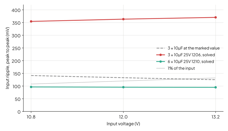
So the miss is 2.6 times at the worst corner, and the worst corner has moved. Fig. 2 shows the shape. On marked values, ripple falls as the input rises. On the 1206 parts it rises, because each extra volt of DC bias costs more capacitance than the falling saves. Check only at minimum input, where the simple estimate says to, and you check the wrong end.
A higher voltage rating doesn't buy the capacitance back. Across 102 vendor curves for 10µF parts in 1206, the 16V and 25V ratings keep the same median fraction at 13.2V, 0.42. A larger case does buy it back: 25V parts in 1210 keep 0.79. The MLCC DC bias derating note explains why the label predicts this badly, and how to estimate it from the dimensions.
The corrected build uses six GRM32DR71E106KA12, the 10µF, 25V X7R part in 1210. They keep 43.5µF of their 60µF at 12V. The ripple is 97mV at 10.8V and 95mV at 13.2V, 0.89% of the input at the worst corner. I aimed for under 1%. Four parts gave 1.34%.
The input capacitors also carry RMS current:
where is the RMS current in the input capacitors, is the 10A load and the duty cycle from step 1. It's 4.61A at 10.8V. Spread across the bank, the solve puts the self-heating at 3.2°C for the three 1206 parts and 1.0°C for the six 1210 parts. That isn't the limit here.
Step 5: output capacitors
The output ripple is set by the inductor ripple and the output capacitance:
where is the peak-to-peak output ripple, the 3.30A inductor ripple at 13.2V from step 2, the switching frequency and the output capacitance.
At 10A the ripple isn't what sizes the output. The load step is. A first estimate of the droop for a step that the loop corrects at its crossover frequency is [6]
where is the output droop, is the load step, is the loop's crossover frequency and is the output capacitance.
With a 5A step, a 50kHz crossover and 3% of 3.3V allowed, that asks for 161µF. Eight 22µF capacitors make 176µF marked, so the simple estimate fits eight and stops.
I used eight GRM21BR60J226ME39, the common 22µF, 6.3V X5R part in an 0805 case. At 3.3V they keep 83.5µF, 47% of the marked value. Part of that is DC bias, because 3.3V is over half the part's rating. The rest is the small AC level of converter ripple, at which a dense ceramic reads below its marked value even with no bias [7]. The droop comes out at about 190mV, against the 99mV target.
The solve doesn't flag any of this. The output ripple is 12mV, well inside any sensible limit, and ripple is the check that's run. The load step needs either 16 of these parts or a larger case. The corrected build uses nine GRM32ER71A226ME20, the 22µF, 10V X7R part in 1210. They keep 187µF, and the droop estimate is 85mV.
Step 6: MOSFETs
At a duty cycle of 0.25 to 0.31, the low-side switch conducts for about 70% of each period. The simple estimate gives it the lowest RDS(on) it can find. I solved twelve pairings of Infineon parts at 12V, three high-side against four low-side. Everything else is as in the corrected build:
| High side | Low side | Low side RDS(on) at 10V | High-side loss | Low-side loss | Efficiency |
|---|---|---|---|---|---|
| BSC024NE2LS | BSC0901NSI | 1.7mΩ | 436mW | 329mW | 95.27% |
| BSC024NE2LS | BSC011N03LSI | 0.9mΩ | 525mW | 310mW | 95.08% |
| BSC024NE2LS | BSC010NE2LS | 0.8mΩ | 684mW | 338mW | 94.57% |
The part with twice the resistance wins. The three low-side losses are 28mW apart at most. The difference turns up in the high side, which loses 248mW more with the BSC010NE2LS underneath it.
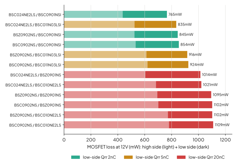
The cause is the low side's body diode. During the dead time before the high side turns on, the low side's body diode carries the load current.
When the high side turns on, it has to sweep out that diode's stored charge at the full input voltage. The energy is dissipated in the high side. The BSC010NE2LS datasheet gives a reverse-recovery charge of 20nC [8]. Infineon describes the BSC0901NSI as having an integrated monolithic Schottky-like diode, and gives 2nC [9]. In the solve, the high side's recovery term is 232mW over the BSC010NE2LS against 24mW over the BSC0901NSI.
So the low side has to be chosen on what it costs the high side as well as on its own loss. The Coss loss note works through the same question for the output capacitance: which switch pays, and how much. The engine does warn that the BSC0901NSI's Qrr was measured at a different junction temperature from this design's. The ranking holds by a wide margin, but the 24mW is the less certain number of the two.
Two things I expected to matter here didn't, much. A 5V gate drive leaves RDS(on) about 1.21 times its 10V headline figure, the median across 52 datasheets. And the old rule of 0.5% per °C for RDS(on) against temperature [10] holds within 10% on all 64 datasheet curves I checked. Neither moves the ranking above. The MOSFET selection article goes further into the trade between resistance and switching loss.
At this ripple it also barely matters which current each switching edge is charged at. The solve charges the high side's turn-on at the inductor's 8.4A valley and its turn-off at the 11.6A peak, not both at the 10A average. The two nearly cancel, and the high side's switching loss moves by 5mW. The edges spread apart as the ripple ratio rises, so a design run at higher ripple can't assume the same.
The two builds side by side
Both builds use the BSC024NE2LS and BSC0901NSI, solved at 50°C ambient:
| Simple estimate | Corrected | |
|---|---|---|
| Inductor | 1274AS-H-1R5N | DD1274AS-H-1R5N |
| Input capacitors | 3 × GRM31CR71E106KA12 (1206) | 6 × GRM32DR71E106KA12 (1210) |
| Output capacitors | 8 × GRM21BR60J226ME39 (0805) | 9 × GRM32ER71A226ME20 (1210) |
| Inductor at 13.2V | 95.0°C, limit 85°C | 95.1°C, limit 105°C |
| Input ripple, worst corner | 370mV at 13.2V | 97mV at 10.8V |
| Output capacitance kept | 83.5µF of 176µF | 187µF of 198µF |
| Load-step droop estimate | about 190mV | about 85mV |
| Efficiency at 12V | 95.21% | 95.27% |
The efficiencies differ by 0.06 points. Every failure in the left-hand column is a part working outside a rating, and efficiency doesn't see any of them. The inductor's loss is the same in both builds. Only its limit changed.
The loop isn't designed here. For a voltage-mode controller it's a Type III network, worked through in Part 2 of the compensator series. For peak current mode it's a Type II, in the current-mode Part 2. The 50kHz crossover in step 5 is the target either one has to meet.
What changes the answer
Every result above depends on things I fixed at the start. At 40°C ambient the 1274AS-H-1R5N passes. On a worst-case DC resistance the DD1274AS-H-1R5N is close to its limit. The input ripple target of 1% is a choice, and at 2% four 1210 parts would do. On a different board, with more copper or airflow, the inductor runs cooler than Murata's test PCB says.
What doesn't change is the method. Each part has a rating defined at one condition, and the design asks it to work at another. The datasheet number that decides the part is rarely the one in the selection table.
Swap any part above and the checks move. A different inductor changes the ripple, which changes the output and the high side's loss. A cheaper input capacitor moves the worst corner. Re-running every check at every corner, each time a part changes or goes out of stock, is what eats a design week. switchmode.io is being built so that a part swap re-grades the whole design before anything reaches the bench.
References
[1] Wevolver, "Buck Converters: A Comprehensive Guide for Hardware Design Engineers," Mar. 31, 2026. [Online]. Available: https://www.wevolver.com/article/buck-converters-a-comprehensive-guide-for-hardware-design-engineers
[2] Murata Manufacturing, "1274AS-H-1R5N=P3," product page. [Online]. Available: https://www.murata.com/en-us/products/productdetail?partno=1274AS-H-1R5N%3DP3
[3] Murata Manufacturing, "DEM10050C Type reference specification," J(E)TE243B-0058, Jul. 2025. [Online]. Available: https://pim.murata.com/asset/pim4/inductor/J(E)TE243B-0058_DEM10050C_REFERENCE_PDF_INDUCTOR
[4] Murata Manufacturing, "DEM10050C(DD) Type reference specification," J(E)TE243B-0063, Jul. 2025. [Online]. Available: https://pim.murata.com/asset/pim4/inductor/J(E)TE243B-0063_DEM10050C(DD)_REFERENCE_PDF_INDUCTOR
[5] Coilcraft, "XAL1010 Series High Current Shielded Power Inductors." [Online]. Available: https://www.coilcraft.com/en-us/products/power/shielded-inductors/molded-inductor/xal/xal1010/
[6] J. Betten, "Power Tips: Calculating capacitance for load transients," Texas Instruments, SSZTCQ4. [Online]. Available: https://www.ti.com/lit/pdf/ssztcq4
[7] Murata Manufacturing, "SimSurfing: design support software for multilayer ceramic capacitors." [Online]. Available: https://ds.murata.com/simsurfing/
[8] Infineon Technologies, "BSC010NE2LS," product page and datasheet. [Online]. Available: https://www.infineon.com/part/BSC010NE2LS
[9] Infineon Technologies, "BSC0901NSI," product page and datasheet. [Online]. Available: https://www.infineon.com/part/BSC0901NSI
[10] D. Schelle and J. Castorena, "Buck-Converter Design Demystified," Electronic Design, Jun. 1, 2006. [Online]. Available: https://www.electronicdesign.com/technologies/power/power-supply/dc-dc-converters/article/21188914/buck-converter-design-demystified