Part 1 showed what a peak current loop does to a buck converter's plant. The LC resonance goes, a single pole at 727Hz takes its place, and the phase at a 50kHz crossover is −95° instead of −170°. That puts the job within reach of a Type II compensator: an integrator, one zero and one high-frequency pole.
This article turns Part 1's targets into component values, twice over. Once around an op-amp, which is how a Type II is usually drawn. Once around a transconductance amplifier, which is what most current-mode controllers actually have. The targets are the same, and the arithmetic isn't. With a transconductance amplifier, the feedback divider lands inside the loop gain.
Design targets (from Part 1)
A 9–36V to 5V, 2A buck at 500kHz, peak current mode, designed at 18V. From Part 1, the plant at 50kHz is −3.76dB and −95.2°.
The compensator targets:
- Crossover frequency : 50kHz, a tenth of the switching frequency
- Phase margin: 60° at 18V
- Phase boost at crossover: 65.2°
- Zero: = 10.98kHz
- High-frequency pole: = 227.7kHz
- Compensator gain at crossover, : +3.76dB, a factor of = 1.542, so that the loop gain is 0dB there
- Feedback divider: 10.5kΩ over 2.00kΩ, both E96 values, giving 5.000V from a 0.8V reference
The zero and pole sit a factor of = 4.55 either side of crossover, so . That symmetric placement gives the most phase boost for a given spacing [3], and it simplifies the arithmetic below.
Two ways to build a Type II
Fig. 1 shows both circuits. The component names follow TI's SLVA662 [1]: and are the divider, and set the zero, and sets the high-frequency pole.
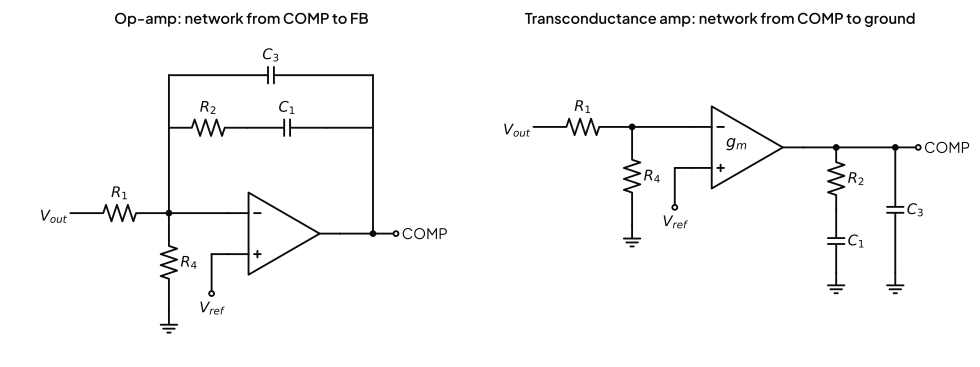
Around an op-amp, the network sits between COMP and the inverting input. Feedback holds the inverting input at the reference, so it's a virtual ground. sets the DC output voltage and drops out of the AC analysis entirely. The compensator is the network impedance over the upper divider resistor:
where is the compensator's gain from the output voltage to the control voltage. is the impedance of the network in the feedback path, in ohms, and is the upper divider resistor.
Around a transconductance amplifier (OTA), there is no local feedback. The amplifier turns its input voltage into a current, and the network to ground turns that current back into the control voltage. With no virtual ground, the divider ratio and the transconductance both land in the gain [1, Eq. 12]:
where is the lower divider resistor and is the amplifier's transconductance, in siemens. , and are as above.
In both cases the network is the same:
where:
- is the complex frequency, in radians per second
- is the resistor in series with , in ohms
- is the capacitor that sets the zero with , in farads
- is the capacitor across that branch, which sets the high-frequency pole, in farads
| Feature | Frequency | Set by |
|---|---|---|
| Zero | , | |
| High-frequency pole | , , | |
| Integrator | , scaled by or by | , |
The design equations
The zero and the pole fix the ratio of the two capacitors. Divide by and cancels:
where is the zero frequency and the high-frequency pole, both in hertz, and both taken from the targets above.
The gain at crossover fixes . Write the network's magnitude at with two correction terms, for the pole and for the zero. With symmetric placement , so = 1.024 and they cancel. Then for the op-amp:
where is the compensator gain needed at crossover, 1.542 here, and is the crossover frequency. and are the two correction terms defined above, and , and are as before.
And for the OTA [1, Eq. 18]:
where and are the divider resistors and the transconductance. , , , and are as above.
The two differ only in what stands in for . In the OTA it is . SLVA662 gives the OTA form directly. Its op-amp section is parameterised differently, so I derived the op-amp expression above and checked it numerically. Everything after that is shared:
where is the value just calculated, in ohms, and and come out in farads.
Worked example: the op-amp version
Step 1: = 10.5kΩ. It's the upper divider resistor, chosen with to set 5V. In an op-amp design it also sets the compensator's gain, so change the output voltage with , not [1].
Step 2: .
Step 3: and .
Worked example: the transconductance version
Step 1: = 350µS. That is the TPS54360B's typical figure [2]. Take it from your own controller's datasheet.
Step 2: . The divider ratio is 0.16, so = 17.86kΩ:
Step 3: and .
I checked both networks by evaluating the circuits themselves rather than the formulas above. Each one lands on Part 1's targets: 50.0kHz crossover, 60.0° of phase margin at 18V.
Rounding to standard values
E96 resistors and E12 capacitors:
| Component | Op-amp exact | Op-amp standard | OTA exact | OTA standard |
|---|---|---|---|---|
| 17.02kΩ | 16.9kΩ | 28.94kΩ | 28.7kΩ | |
| 851.9pF | 820pF | 500.9pF | 470pF | |
| 43.16pF | 47pF | 25.38pF | 27pF |
The resistors barely move. The capacitors do the damage, and they do it in the unhelpful direction. rounds down, which raises the zero. rounds up, which lowers the pole. On the OTA version the zero moves from 10.98kHz to 11.80kHz and the pole from 227.7kHz to 217.2kHz. The spacing shrinks from 4.55 to 4.29, and the boost falls from 65.2° to 63.8°.
That costs 1.3° of phase margin at every input voltage. I expected rounding to be free here, because the Type III in the voltage-mode Part 2 came out a degree better after rounding. It doesn't work that way. In that design the errors pulled against each other. Here both capacitors move the zero and the pole the same way.
It isn't a large loss, and it is avoidable. With E24 capacitors, 510pF and 24pF, the OTA version lands at 60.8° at 18V. The op-amp version takes 820pF and 43pF and lands at 59.6°. E24 values are easy to buy in C0G, the dielectric you want here anyway.
Verification
Fig. 2 shows the E12 networks on Ridley's plant at 18V.
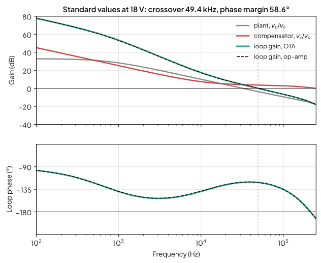
At all three input corners, with E12 values:
| 9V | 18V | 36V | |
|---|---|---|---|
| Op-amp: crossover, PM, GM | 49.9kHz, 61.8°, 13.8dB | 49.3kHz, 58.7°, 15.3dB | 49.0kHz, 57.2°, 15.9dB |
| OTA: crossover, PM, GM | 50.0kHz, 61.7°, 13.8dB | 49.4kHz, 58.6°, 15.3dB | 49.0kHz, 57.1°, 15.9dB |
The crossover moves by 1kHz across a 4:1 input range, which is the current-mode property Part 1 set out. The gain margin comes from the sampling pole at half the switching frequency, which is where the loop phase finally passes −180°.
Two things an OTA does that an op-amp doesn't
The divider is in the loop. Change the output voltage with the op-amp design by changing , and the compensator's gain at crossover doesn't move. Do the same with the OTA design and it does. Moving this converter to 3.3V takes from 2.00kΩ to 3.36kΩ. The op-amp's gain at 50kHz stays at 1.52. The OTA's rises to 2.31, 3.6dB more, because the divider now passes a bigger fraction of the output to the amplifier.
SLVA662 puts it plainly: with an OTA, "only the ratio of the feedback resistors is important" [1, p. 3]. That also means the ratio is part of your compensation. Change the output voltage on an OTA design and redo .
is a gain you don't control. In the op-amp version, the gain is a ratio of two resistors you chose. In the OTA version it is proportional to , which is set inside the chip. The TPS54360B datasheet gives a typical value only [2]. If is 20% off, on the standard-value OTA network at 18V:
| Crossover | Phase margin | Gain margin | |
|---|---|---|---|
| 280µS (−20%) | 40.1kHz | 59.4° | 17.2dB |
| 350µS | 49.4kHz | 58.6° | 15.3dB |
| 420µS (+20%) | 58.6kHz | 57.0° | 13.7dB |
The phase margin barely moves, because the plant phase is flat near crossover. The crossover does move, and with it the load-step response. Check your part's limits before you promise a transient spec.
The OTA's finite gain matters much less. The TPS54360B's 10,000V/V turns the ideal integrator into a pole at 11Hz, far below anything that affects the margins.
What comes next
Every number here assumes the compensating ramp that Part 1 chose, 0.67 times the inductor downslope, without justifying it. Part 3 is about that choice. It covers how much ramp a peak current-mode buck needs, and what too little and too much cost. It also explains why the margins in the table above still drift across the input range.
The algebra above is the easy part, and it is the part every application note covers. What costs time on a real design is everything after it. Round to the parts you can buy, re-grade at every input corner, then do it again when the inductor or the controller changes. That is the part switchmode.io automates.
References
[1] S. W. Lee, "Demystifying Type II and Type III Compensators Using Op-Amp and OTA for DC/DC Converters," Texas Instruments, Application Report SLVA662, Jul. 2014. [Online]. Available: https://www.ti.com/lit/an/slva662/slva662.pdf
[2] Texas Instruments, "TPS54360B 4.5-V to 60-V Input, 3.5-A Step-Down DC-DC Converter," SNVSB93, Dec. 2018. [Online]. Available: https://www.ti.com/lit/ds/symlink/tps54360b.pdf
[3] H. D. Venable, "The K factor: A new mathematical tool for stability analysis and synthesis," Proc. Powercon 10, San Diego, CA, 1983. [Online]. Available: https://www.venableinstruments.com/hubfs/The%20K%20Factor%20a%20New%20Mathematical%20Tool%20for%20Stability%20Analysis.pdf