A voltage-mode buck needs a Type III compensator for one reason. Its inductor and output capacitor form a resonant double pole. By any useful crossover frequency, that pole has dragged the phase to nearly −180°. The voltage-mode version of this problem works through why.
Put the same inductor inside a current loop and most of that problem goes away. The plant becomes a single pole, and a two-zero compensator is no longer needed. Most of it goes away. The inductor doesn't vanish. It reappears as a pole at half the switching frequency. Ignore it and a converter can oscillate at 43% duty while its averaged-model Bode plot looks perfectly healthy.
This article covers what the current loop does to the plant, why it needs a ramp, and what the compensator has to do. Part 2 calculates every component value. Part 3 asks how much ramp to use across the whole input range.
The worked example
A 9–36V to 5V buck converter at 2A, switching at 500kHz, using peak current-mode control.
Power stage components:
- Output inductor: 14.35µH, sized for 30% ripple at 36V
- Output capacitance: 100µF, 5mΩ effective ESR
- Load: 2.5Ω (2A at 5V)
- Current-sense gain : 0.05V/A, from sense resistor to comparator
- Feedback reference: 0.8V
- Duty cycle: 0.139 at 36V, 0.278 at 18V, 0.556 at 9V
The compensator is designed at 18V, the middle of the range, and checked at both ends. The compensating ramp is 11,700V/s, which is 0.67 times the inductor downslope as the comparator sees it. Part 3 is about why that number and not another. For now, take it as given.
How peak current mode closes the inner loop
A clock pulse turns the switch on at the start of every period. The inductor current ramps up, and a sense resistor turns it into a voltage. A comparator watches that voltage, plus the compensating ramp, and turns the switch off when it reaches the control voltage .
The error amplifier sets . So the voltage loop no longer commands a duty cycle. It commands a peak inductor current, cycle by cycle, and the comparator works out the duty that delivers it.
That makes two loops. The inner current loop runs at the switching frequency and needs no compensator. The outer voltage loop is the one you design, and the current loop has changed what it sees.
What the current loop does to the plant
Fig. 1 plots the control-to-output transfer function for the same power stage twice. Once in voltage mode, with a 1V PWM ramp. Once in peak current mode, with the ramp above.
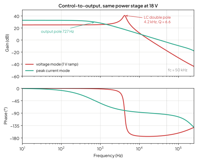
In voltage mode the inductor and capacitor resonate at 4.2kHz with a Q of 6.6. The phase collapses through that resonance and sits at −170° at 50kHz.
In current mode the error amplifier sets the inductor current directly. The inductor stops behaving like an energy store that can ring with the capacitor. It behaves like a controlled current source feeding the capacitor and load in parallel. What remains is one pole, at roughly :
For this converter is 637Hz. Ridley's more complete model moves it to 727Hz and lowers the DC gain slightly, to 32.8dB [2, Eq. 5.8]. The capacitor's ESR zero is at 318kHz in both modes, too high to help. At 50kHz the current-mode plant has −95° of phase against −170° in voltage mode. That difference is the whole reason current mode gets away with a simpler compensator.
There's a second benefit, and it's easy to miss. Above the output pole the gain simplifies to . The load resistance has dropped out, and so has the input voltage. In voltage mode the plant gain scales with , so a 4:1 input range moves the crossover. In current mode it doesn't. That matters for a 9–36V design, and it comes back at the end of this article.
Where the inductor went: a pole at half the switching frequency
The single-pole picture is the averaged model, and it has a limit. Erickson and Maksimović are explicit about it. Switching and sampling produce effects "not predicted by the continuous-time averaged analysis". So "the averaged model is valid only at frequencies sufficiently less than one-half of the switching frequency" [1, p. 468].
The comparator samples the inductor current once per cycle. Ridley showed that this sampling puts a double pole at half the switching frequency, with a quality factor set by the ramp [2, Eq. 5.12]:
is the sensed on-slope and the compensating ramp, both in volts per second at the comparator. With this converter's ramp, is 0.78 at 18V.
That pole is where the inductor went. It costs 15° of phase at a 50kHz crossover, and 31.5° at 100kHz. It is why current-mode crossover still sits near a tenth of the switching frequency. The low-frequency plant alone would allow more.
Why the current loop needs a ramp
The ramp exists because the inner loop can go unstable on its own. Disturb the inductor current at the start of a cycle and the comparator trips at a different time. With no ramp, the disturbance at the start of the next cycle is multiplied by [1, Eq. 12.12]. Above 50% duty that is bigger than one, and each cycle's error grows.
Adding a ramp of slope changes the multiplier to [1, Eq. 12.25]:
where and are the inductor's rising and falling slopes. Enough ramp keeps below one at every duty cycle.
The textbook boundary is 50%. With the voltage loop closed, the real one is lower. As duty approaches 50%, climbs and the pole at peaks. With no ramp, is 6.4 at 45% duty. That is 16dB of extra loop gain at half the switching frequency. It can eat the voltage loop's gain margin while the current loop is still stable.
Erickson flags the gap himself. He calls his stability analysis "a quasi-static approximation". A complete system, he says, "must be assessed using a system-wide discrete time or sampled-data analysis" [1, p. 448].
So I ran one. It's a switched model of this converter, integrated exactly over every on-time and off-time. It includes the inductor, the output capacitor, the comparator and the Type II this article ends up with. Then I took the ramp away.
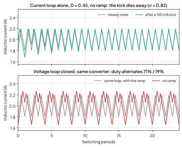
The current loop on its own is stable at 45%. The converter isn't. The small-signal model puts the gain margin at −0.7dB and predicts oscillation from 44.6% duty. The switched model starts oscillating at 42.9%. With the ramp restored, both traces settle.
How much ramp is enough, and what too much costs, is Part 3. The point here is that the ramp is part of the plant. It sets , and sets how much phase the voltage loop loses near crossover.
What the compensator needs to do
It needs an integrator. Without one, the output settles with a steady-state error that changes with load. An integrator gives unlimited gain at DC and removes that error.
An integrator alone isn't enough. It adds −90° everywhere. The plant already sits near −95° well above its output pole. Together that is −185° at 50kHz, a phase margin of −5°. To get 60° with an integrator alone, the crossover has to drop below the output pole, to 419Hz.
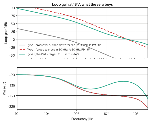
One zero buys the phase back. A Type II compensator is an integrator plus a zero plus a high-frequency pole. The zero sits below crossover and lifts the phase. The pole sits above crossover and rolls the gain off again, so switching ripple doesn't reach the comparator. For 60° at 50kHz, the compensator has to supply 65.2° of boost.
That is within reach, just. With its pole held at , a Type II can supply at most 67.4° at a tenth of the switching frequency. I work through that ceiling in Compensator Types: Choosing Between Type I, II and III. The voltage-mode plant, by comparison, would need 140° of boost at the same crossover. That takes two zeros and a Type III.
Fig. 4 shows what the difference is worth. It is the same switched model, stepping the load from 1A to 2A at 18V.
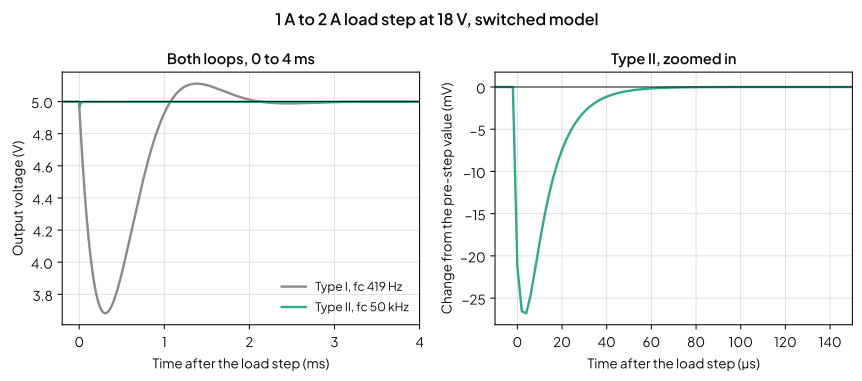
The Type I result isn't a real design. It's the baseline that shows what the zero is for. The Type II dip is close to what the crossover predicts on its own: is 32mV for this converter, against 27mV in the simulation. That estimate is worth remembering. In current mode, the output capacitor and the crossover frequency set the load-step dip. The compensator's job is to get the crossover there with enough phase.
Neither loop hits a duty limit during the step. The Type II duty peaks at 0.53 and the Type I at 0.28, so both responses are small-signal behaviour, not saturation.
Across the input range
Because the plant gain above the output pole doesn't depend on , one compensator designed at 18V holds almost the same crossover everywhere:
| 9V | 18V | 36V | |
|---|---|---|---|
| Crossover | 50.6kHz | 50.0kHz | 49.6kHz |
| Phase margin | 63.1° | 60.0° | 58.5° |
| Gain margin | 13.7dB | 15.3dB | 15.9dB |
That is a 1kHz spread in crossover over a 4:1 input range. A voltage-mode loop on the same range would see its plant gain change by 12dB. The margins still move a little, because moves with duty. Phase margin and gain margin also move in opposite directions. Part 3 is about exactly that, and what the ramp can do about it.
Setting up the targets for Part 2
The Type II has to deliver:
| Target | Value |
|---|---|
| Crossover frequency | 50kHz, a tenth of the switching frequency |
| Phase margin at 18V | 60° |
| Phase boost at crossover | 65.2° |
| Zero | 10.98kHz |
| High-frequency pole | 228kHz |
| Zero-to-pole spacing | = 4.55 either side of crossover |
| Feedback divider | 0.8V reference from a 5V output |
The zero and pole sit symmetrically about crossover, at and , which is the placement that gives the most boost for a given spacing. Part 2 turns them into resistor and capacitor values, the way the voltage-mode Part 2 did for a Type III.
Current mode doesn't make compensation trivial. It swaps a resonant double pole you have to fight for a single pole you can work with. It also adds a sampling pole you have to respect. This analysis is exactly what switchmode.io is being built to do. It runs Ridley's model with the ramp you actually have, and grades one compensator's margins at every corner of the input range.
References
[1] R. W. Erickson and D. Maksimović, "Current programmed control," in Fundamentals of Power Electronics, 2nd ed. Norwell, MA, USA: Kluwer Academic, 2001, ch. 12, pp. 439–487.
[2] R. B. Ridley, "A New Small-Signal Model for Current-Mode Control," Ph.D. dissertation, Virginia Polytechnic Institute and State University, Blacksburg, VA, USA, 1990. [Online]. Available: https://ridleyengineering.com/images/current_mode_book/CurrentModeControl.pdf