Every time a hard-switched half-bridge turns on, the switch output capacitances cost you energy. This note calculates how much, from the datasheet, and says which switch dissipates it. It covers a synchronous buck, a synchronous boost, or any half-bridge that switches hard on at least one edge.
The switch that turns on dissipates its own stored energy. It also dissipates part of the energy it spends charging the other switch. The other switch dissipates nothing capacitive. For two switches that are the same, the total per cycle is , not or . The common estimates put the loss in the wrong switch, get the total wrong, or both.
The result
Call the switch that turns on hard the control switch, and the one on the other side of the switch node the rectifier. Per switching cycle, the control switch dissipates
and the rectifier dissipates no capacitive loss at all. is the voltage the switch node swings through: the input in a buck, the output in a boost. and are the charge and energy stored in each switch's output capacitance at that voltage. The power is
and all of it goes in the control switch's thermal budget. EPC states this split in AN030 [1]. Kasper et al. give the symmetric case, and point out that it's the charge, not the energy, that sets the hard-switching loss [2].
For two switches that are the same, the terms cancel and
Why the rectifier's charge counts, and its energy doesn't
In a buck, the high-side switch is the control switch. Before it turns on, the switch node sits at 0 V and the inductor current flows in the low-side switch. When the high side turns on, the node rises to the input. Two things happen at once, and both go through the high-side channel.
- The high side's own output capacitance discharges from to 0 V, through its own channel. All of its stored energy, , becomes heat.
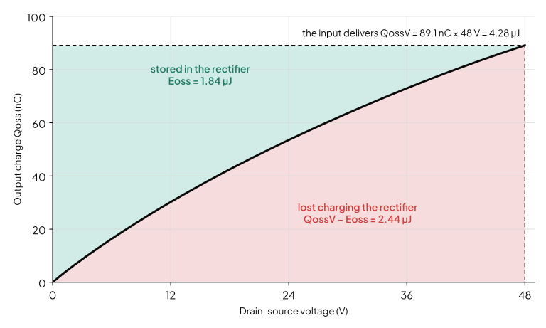
- The low side's output capacitance charges from 0 V to , from the input, through the high-side channel. The input delivers . Only stays stored. The rest becomes heat in the channel.
At the next edge the high side turns off, and the inductor current moves the node back down. That edge is lossless for the capacitances. The inductor charges the high side's capacitance and takes back the energy stored in the low side's. So the low side turns on at close to 0 V, with its body diode already conducting, and it has no capacitive loss. That holds as long as the inductor current can move the node inside the dead time. Step 1 gives the check.
The charge is what counts because the input delivers charge at a fixed voltage. The energy it delivers is whatever shape the capacitance curve has. The energy stored is always less, because the capacitance is largest at low voltage, where each coulomb stores little energy. Fig. 1 shows the areas.
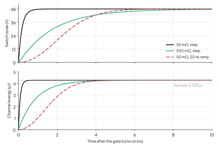
As a numerical check of the energy balance, I simulated the turn-on of two ISC040N10NM7 switches on 48 V with their real curves. The channel was an ideal resistor with no loop inductance. With 50 mΩ or 500 mΩ, and with a step or a 20 ns ramp on the gate, the channel dissipated 4.278 µJ each time. The formula gives 4.278 µJ. The edge speed changes, but the energy doesn't. With 16.7 A of load current, the channel dissipates more, but the extra is exactly the load current's overlap and conduction loss. The capacitive part stays at 4.277 µJ.
What you need from the datasheet
You need and for both switches, at the node voltage. Datasheets give them in four different forms. In order of preference:
- and curves against . Read both off at your voltage. Many SiC and GaN datasheets publish them.
- The curve. Integrate it, as in Step 2 below. This is the usual case for low-voltage silicon.
- and . These are fixed capacitances that store the same energy and the same charge as over a stated range. That's often 0 V to 400 V, or 0 V to 80% of the rated voltage. They give you and at the end of that range only. At any other voltage, go back to the curve.
- A single at one test voltage. Use it only if your voltage is close to the test voltage. Scaling it in proportion to voltage assumes a constant capacitance. On the worked example's switch, 91 nC at 50 V scales to a figure 18% low at 24 V. At 80 V it's 23% high.
Don't use the value from the table. It's a small-signal value at one voltage, and it's the lowest capacitance the switch shows on the way up to that voltage.
Step 1 Find the control switch and the rectifier
The control switch is the one that turns on while the switch node is at the far rail. The rectifier is the one whose body diode is conducting at that moment.
| Converter | Control switch | Rectifier |
|---|---|---|
| Synchronous buck | High side | Low side |
| Synchronous boost | Low side | High side |
| Buck or boost with a diode | The switch | The diode. Use its junction charge and energy in place of and |
Then check that the other edge really is soft. The inductor current at the control switch's turn-off has to move both capacitances through the full swing before the rectifier turns on:
In a buck or a boost, the control switch turns off at the peak inductor current, so use that. Take as the time from the control switch's channel turning off to the rectifier's turn-on. The switch's own turn-off delay uses up part of the programmed dead time. Add any other capacitance on the node, such as a snubber capacitor, to the right-hand side.
If the check fails, the rectifier turns on with voltage still across it, and it dissipates the energy left in the node. That happens at light load. In the worked example the two switches hold 178 nC at 48 V. At 16.7 A the node takes 10.7 ns to fall, and at 8 A it takes 22 ns. Compare that with your controller's dead time.
Count switches in parallel as one. Two rectifier switches in parallel have twice the charge and twice the energy. Two control switches in parallel dissipate the same total, but the split between them depends on which one turns on first.
Step 2 Get Qoss and Eoss at the node voltage
From a curve, integrate:
Digitise the curve, then sum it with the trapezoidal rule. You don't need many points. On the worked example's switch, 25 evenly spaced points to 48 V land in 0.1% of a fine integral of the same curve. Reading a log-scale plot is the bigger error. So check the result against the datasheet's own at its test voltage. They should agree to a few per cent. If they don't, one of them has been read wrongly.
Step 3 Calculate the loss and put it in the control switch
Add it to the control switch's switching loss. Add nothing capacitive to the rectifier, if the check in Step 1 passed.
Step 4 Check you haven't counted it twice
Two datasheet figures can already contain this energy.
- Measured switching energies. and from a double-pulse test carry the capacitive energy between them. includes the charge drawn by the other switch. The tested switch's own discharges inside it, so its energy shows up in as stored energy. If your loss model uses , don't add as well. Infineon builds its SiC simulation models from double-pulse data. It tells you to subtract from the turn-off energy for soft switching [3]. The EPFL group recommends that be published in two parts, one for the output capacitance and one for the load current [4]. Until it is, use with a loss model built from the switching times.
- Reverse recovery charge. On some silicon parts, the datasheet is measured with the output charge included [5], [6]. Then and count the same coulombs. Read the test conditions of before you add both.
Worked example
A 200 W buck: 48 V to 12 V at 500 kHz. It has an Infineon ISC040N10NM7 in both positions. RC Snubber Design uses the same converter. The curve is from the switchmode.io component catalogue, extracted from the datasheet [7]. The datasheet gives no , or , so integrate.
- Roles. The high side is the control switch, and the low side is the rectifier. The falling edge needs 178 nC, which 16.7 A moves in 10.7 ns. Set the dead time longer than that at full load.
- Integrate. (48 V) = 89.1 nC and (48 V) = 1.84 µJ. Check: the integral to 50 V is 91.5 nC, against the datasheet's 91 nC.
- Loss. = 1.84 µJ + 89.1 nC × 48 V − 1.84 µJ = 4.28 µJ. At 500 kHz that's 2.14 W, all in the high side.
- Double counting. This is a model built from switching times, so there's no measured to overlap with.
2.14 W is a lot for the high side. At 25% duty and 16.7 A, its conduction loss is only 0.25 W at the typical of 3.6 mΩ at 25 °C. At the 4.0 mΩ maximum, raised by half for a hot junction, it's 0.42 W. The capacitive loss is five to nine times larger. It sets the high side's temperature in this converter.
Here's how the common estimates compare. Each formula comes from a vendor application note.
| Estimate | Formula from | High side | Low side | Total | Total ÷ correct |
|---|---|---|---|---|---|
| in each switch | Infineon's FAQ [8] | 0.92 W | 0.92 W | 1.84 W | 0.86 |
| in each switch | TI SLPA009A, Eqs. 34–35 [9] | 1.07 W | 1.07 W | 2.14 W | 1.00 |
| in the high side only | Fairchild AN-6005 [5], ROHM 64AN035E [10] | 0.70 W | 0 | 0.70 W | 0.33 |
| This note | EPC AN030 [1] | 2.14 W | 0 | 2.14 W | 1.00 |
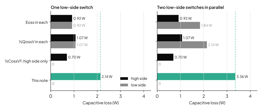
The half- split gets the total right, but only because the two switches are the same part. It still puts half the loss in the low side, so the high side runs hotter than its budget says.
Now parallel two switches on the low side, a common step when the duty cycle is low. The rectifier's charge doubles, and so does its stored energy.
- = 1.84 µJ + 178.3 nC × 48 V − 3.68 µJ = 6.72 µJ, so 3.36 W, all in the high side.
- The half- split gives the high side 1.07 W and the low-side pair 2.14 W. The high side's figure is now three times too low. The total is only 4% low, so the efficiency figure still looks right while the thermal design is wrong.
The second low-side switch saves 0.38 W of conduction loss at the typical . It costs the high side 1.22 W. At full load that's a net loss of 0.84 W, and all of it lands on the switch that was already the hottest. Budget for it before you parallel.
How far the common estimates are out
For two switches that are the same part, the correct loss is . The table shows how far the two most common estimates fall short of it. The -per-switch estimate gives . The high-side-only estimate gives . The shortfall depends on the technology and on how far up its rating the voltage sits.
| Part | Technology | Voltage | ||
|---|---|---|---|---|
| ISC040N10NM7 | 100 V trench silicon | 24 V | 1.10 | 2.54 |
| ISC040N10NM7 | 100 V trench silicon | 48 V | 1.16 | 3.07 |
| ISC040N10NM7 | 100 V trench silicon | 80 V | 1.29 | 4.50 |
| BSC009N04LSSC | 40 V trench silicon | 32 V | 1.44 | 4.88 |
| IMBG65R057M1H | 650 V SiC | 400 V | 1.32 | 3.01 |
| IMBG65R050M2H | 650 V SiC | 400 V | 1.48 | 3.57 |
| IPA60R180P7 | 600 V superjunction | 400 V | 10.5 | 40 |
The silicon and SiC figures come from integrating each part's catalogue curve. The superjunction figures come from the datasheet's = 36 pF and = 381 pF over 0 V to 400 V [11].
The superjunction row is one reason superjunction switches aren't used in hard-switched half-bridges. The body diode's reverse recovery is the other. Two IPA60R180P7s at 400 V would dissipate 61 µJ per cycle, which is 6.1 W at 100 kHz. The -per-switch estimate says 0.58 W. Now use the same part as a single boost switch, with a SiC diode as the rectifier. It pays its own of 2.9 µJ, plus the diode's . Take that from the diode's datasheet. It isn't always small next to 2.9 µJ.
Assumptions and limits
- Hard switching only. The formula assumes the control switch turns on with the node at the far rail. If the inductor current reverses during the dead time, as it can at light load in forced-continuous mode, it moves the node for you. Then the edge is partly or fully soft, and the loss falls. With enough reverse current, the control switch turns on at 0 V and dissipates nothing capacitive [2].
- The rectifier's edge must be soft. The check in Step 1 has to pass. At light load it often doesn't, and then the rectifier dissipates what's left in the node when it turns on.
- The datasheet curve is a small-signal measurement. Some superjunction, SiC and GaN parts take a different charge-voltage path up than down. This hysteresis loses energy on every cycle, and the curve can't show it [4], [12], [13]. Some of that loss may land on the soft edge, and the datasheet can't tell you how much. On those parts, treat this note's figure as a lower bound, and the rectifier's zero as optimistic.
- Other capacitance on the switch node counts too. The inductor's winding capacitance charges through the control switch. So do the PCB and any Schottky across the low side. Add each one's charge and energy to the rectifier's. A bare linear capacitor adds per cycle to the control switch [5]. An RC snubber costs up to per cycle, and the control switch takes at most of it. The resistor takes the rest. Count the snubber capacitor's charge in the Step 1 check as well.
- The gate-drain part of . includes , and its current flows partly through the gate loops. So a small part of the energy lands in the gate resistors and drivers, not the channel. The total is the same. On the worked example's switch, is 13 pF of the 1,170 pF at 50 V [7].
- Only the capacitive term. Overlap loss, reverse recovery, gate drive and conduction are separate terms. The load current adds overlap loss to the same edge.
What this means for switchmode.io
The MOSFET power loss calculator uses this split. It reads each switch's , and curves from the component catalogue at your operating voltage. It puts the whole capacitive loss in the control switch. When the other switch publishes no capacitance data, it says so instead of guessing. It also solves each junction temperature against its own loss, which is what decides whether the high side survives the watts this note finds.
For the other loss terms in a buck, see The Buck Converter Losses Nobody Tells You About. A low-side choice can cost the high side watts through too. Why the Lowest RDS(on) Isn't the Best MOSFET for Your Buck Converter makes that point.
References
[1] A. Gorgerino, "Hard switching losses calculations," EPC Application Note AN030, 2024. [Online]. Available: https://epc-co.com/epc/portals/0/epc/documents/application-notes/AN030%20Hard%20Switching%20Losses%20Calculation.pdf
[2] M. Kasper, R. M. Burkart, G. Deboy and J. W. Kolar, "ZVS of power MOSFETs revisited," IEEE Trans. Power Electron., vol. 31, no. 12, pp. 8063–8067, Dec. 2016. [Online]. Available: https://www.ams-publications.ee.ethz.ch/uploads/tx_ethpublications/5_ZVS_of_Power_MOSFETs_Revisited_Kasper_01.pdf
[3] Infineon Technologies, "Understanding and interpreting the CoolSiC MOSFET 1200 V datasheet," Application Note AN2025-10, V1.1, Jul. 2026. [Online]. Available: https://www.infineon.com/assets/row/public/documents/60/42/infineon-an2025-10-understanding-and-interpreting-the-coolsic-mosfet-1200v-datasheet-applicationnotes-en.pdf
[4] E. Matioli, H. Zhu, N. Perera, M. Samizadeh Nikoo, A. Jafari and R. van Erp, "Switching losses in power devices: From dynamic on resistance to output capacitance hysteresis," PECTA contribution, EPE 2023. [Online]. Available: https://www.iea-4e.org/wp-content/uploads/publications/2023/10/594_full_paper_pdf.pdf
[5] J. Klein, "Synchronous buck MOSFET loss calculations with Excel model," Fairchild Semiconductor Application Note AN-6005, 2006. [Online]. Available: https://www.bdtic.com/datasheet/fairchild/AN-6005.pdf
[6] Nexperia, "Understanding power MOSFET data sheet parameters," Application Note AN11158. [Online]. Available: https://assets.nexperia.com/documents/application-note/AN11158.pdf
[7] Infineon Technologies, "ISC040N10NM7 OptiMOS 7 power MOSFET 100 V," datasheet, rev. 1.0, Nov. 2025. [Online]. Available: https://www.infineon.com/assets/row/public/documents/24/49/infineon-isc040n10nm7-datasheet-en.pdf
[8] Infineon Technologies, "FAQ: MOSFET output capacitance (Coss)," Knowledge Base Article, Apr. 2025. [Online]. Available: https://community.infineon.com/t5/Knowledge-Base-Articles/FAQ-MOSFET-Output-Capacitance-Coss/ta-p/374758
[9] D. Jauregui, B. Wang and R. Chen, "Power loss calculation with common source inductance consideration for synchronous buck converters," Texas Instruments Application Report SLPA009A, Jul. 2011. [Online]. Available: https://www.ti.com/lit/an/slpa009a/slpa009a.pdf
[10] ROHM Semiconductor, "Efficiency of buck converter," Application Note 64AN035E, rev. 004, Nov. 2022. [Online]. Available: https://fscdn.rohm.com/en/products/databook/applinote/ic/power/switching_regulator/buck_converter_efficiency_app-e.pdf
[11] Infineon Technologies, "IPA60R180P7 600V CoolMOS P7 power transistor," datasheet, rev. 2.2, Oct. 2017.
[12] J. B. Fedison, M. Fornage, M. J. Harrison and D. R. Zimmanck, "Coss related energy loss in power MOSFETs used in zero-voltage-switched applications," in Proc. IEEE APEC, 2014, pp. 150–156.
[13] J. B. Fedison and M. J. Harrison, "COSS hysteresis in advanced superjunction MOSFETs," in Proc. IEEE APEC, 2016, pp. 247–252.