Your switch node rings because the power loop's inductance resonates with the capacitance across the switch. An RC snubber damps that ring by turning its energy into heat. This note takes you from a ringing waveform on the scope to a resistor, a capacitor and a dissipation figure. It ends with a worked example and a check on the bench.
Three things here aren't in the usual references. The added-capacitor measurement has an error budget, and the capacitor you add decides how big it is. The ring follows the switch's output capacitance at your bus voltage, not the charge-equivalent value. And the resistor has a published closed-form optimum that tolerates a wide spread, but the common rule of half the characteristic impedance falls outside it.
Before you start: is a snubber the right fix?
A snubber doesn't remove the ringing energy. It burns it, every cycle. The snubber capacitor charges to the bus voltage and discharges again on each switching cycle. Budget its cost as
That doesn't depend on the resistor [1], [2]. A 2.2 nF snubber on a 48 V bus switching at 500 kHz costs up to 2.5 W. Treat it as an upper bound on the total.
Todd notes the estimate runs high when the snubber's time constant is comparable with the switching edge [1]. And part of the charging loss lands in the switch that drives the edge, not in . So it also belongs in that switch's thermal budget. It's a loss term like any other, next to the ones in The Buck Converter Losses Nobody Tells You About.
The ring is set by your layout. Its frequency and its characteristic impedance both come from the loop inductance. Halving the loop inductance cuts the characteristic impedance by √2. That cuts the spike the switched current drives across the node, and it costs no watts. So fix the layout first.
PCB Layout for Switchmode Converters works through the same 48 V bus at loop inductances from 2 nH to 20 nH. Reach for a snubber when the layout is as good as it will get and the ring still costs you voltage margin or EMI.
What you need
- A scope and probe with at least 500 MHz of bandwidth [2]. The ring in the worked example is at 65 MHz, and a GaN switch in a tight layout can ring above 100 MHz.
- A short ground connection. Use the ground spring, or a differential probe. TI measured 21.76 V with a single-ended probe on a 6.5-inch ground lead. At the same test condition, a differential probe read 18.4 V [2].
- A C0G capacitor to add, roughly three times the switch's output capacitance, with a 1% or 2% tolerance. Step 2 explains the size.
- The circuit running at its real bus voltage. The switch's output capacitance falls as the voltage rises, so the ring frequency changes with the bus. Check the setup at a reduced voltage first if you like [1], but take the measurements at your operating voltage.
Step 1 Measure the ring frequency
Probe the switch node right at the low-side switch's drain and source. In a buck, the ring to measure follows the high-side switch's turn-on, when the node rises to the bus. Trigger on that edge.
Skip the first overshoot, then measure across several periods and divide. The first cycle swings further than the rest and runs a few percent slower. Averaging over several periods also cuts the error of reading one period with cursors.
This is , the frequency of the loop inductance against the node capacitance :
You don't know or yet. One measurement gives one equation, which is why step 2 exists.
Step 2 Add a known capacitor and measure again
Solder a known capacitor across the low-side switch, as close to its pins as you can. The ring slows to
Divide the two equations and square them. With :
which rearranges to
Nexperia AN11160 derives the same result in its Appendix A [3]. includes the probe, which the next section removes.
Be quick with this step. The added capacitor has no resistor, so the high-side switch charges it through its own channel every cycle. A 3.3 nF capacitor at 48 V and 500 kHz adds 1.9 W to that switch, plus a bigger turn-on current spike. At light load, where the inductor current can't discharge it in the dead time, it adds up to another 1.9 W to the low side. Run at light load or a reduced switching frequency, keep the full bus voltage, and watch the switch's temperature.
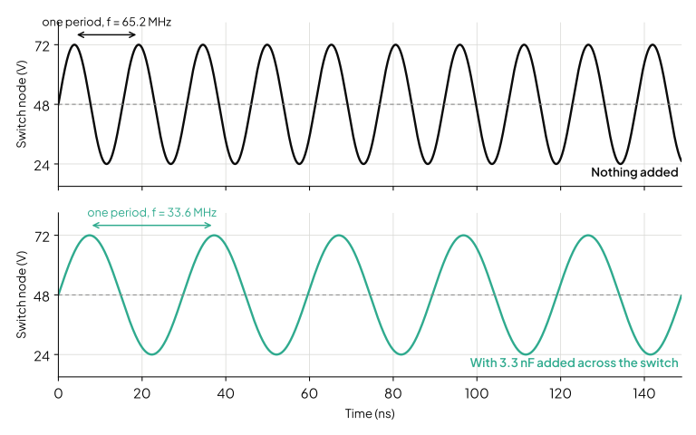
How big should the added capacitor be?
Big enough to roughly halve the frequency, which means about three times . The reason is the error budget, and I haven't seen it published anywhere.
Differentiate , and a small error in the frequency ratio becomes
The multiplier grows without limit as approaches 1, so a small added capacitor amplifies every reading error. If each frequency is read to 1%, the ratio can be out by 2%, and that costs:
| Added capacitor | Frequency ratio | Error in , each frequency read to 1% | ... read to 2% |
|---|---|---|---|
| 0.25 | 1.12 | 20% | 40% |
| 0.5 | 1.22 | 12% | 24% |
| 1 | 1.41 | 8.0% | 16% |
| 2 | 1.73 | 6.0% | 12% |
| 3 | 2.00 | 5.3% | 11% |
| 10 | 3.32 | 4.4% | 8.8% |
The added capacitor's own tolerance passes straight into as well, so add it to these figures.
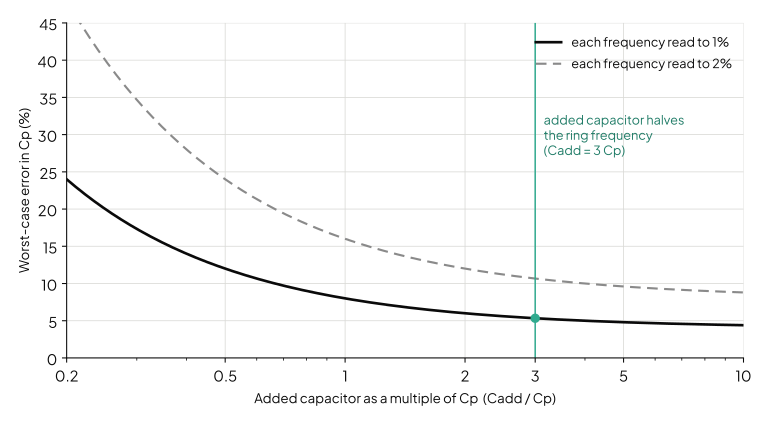
You don't know before you start, so use the datasheet's output capacitance as the first guess (step 3 explains which figure). If the frequency falls by less than about 30%, add more capacitance and measure again.
Correct for the probe
The probe tip adds its own capacitance to the node, so is . Work in this order:
- , using , because was measured with the probe on
- , the characteristic impedance you'll need in step 5
A 500 MHz 10× passive probe such as Tektronix's TPP0500B adds under 4 pF [8]. That's 0.3% of a 100 V silicon switch's 1.2 nF, but 4% of a 100 pF GaN device. A 10 pF probe would make it 10%. Use the tip capacitance from your probe's datasheet.
Step 3 Check Cp against the datasheet
Your should be close to the switch's output capacitance, , at your bus voltage. Most of any difference is stray capacitance on the node.
It's worth being precise about which datasheet figure, because changes a lot with voltage. On the part in the worked example, the fitted curve falls about four times between 0 V and 100 V. A datasheet can quote three different numbers:
- on the front page, a small-signal value at one test voltage, usually half the rating. It's usually the typical value, and the maximum can be 30% higher, which is one more reason to measure.
- , the energy-equivalent capacitance, which stores the same energy as the real curve when charged to a given voltage.
- , the charge- or time-equivalent capacitance, which takes the same charge and so the same time to charge at constant current. Kasper et al. show it's the one that matters for ZVS and for hard-switching loss [4].
Once the node has switched, the ring swings around the bus voltage, so it sees the capacitance at the bus voltage. I simulated the ring on the Infineon ISC040N10NM7's curve, fitted to its published and [7], with a 5 nH loop. The part doesn't publish or , so both come from the fitted curve.
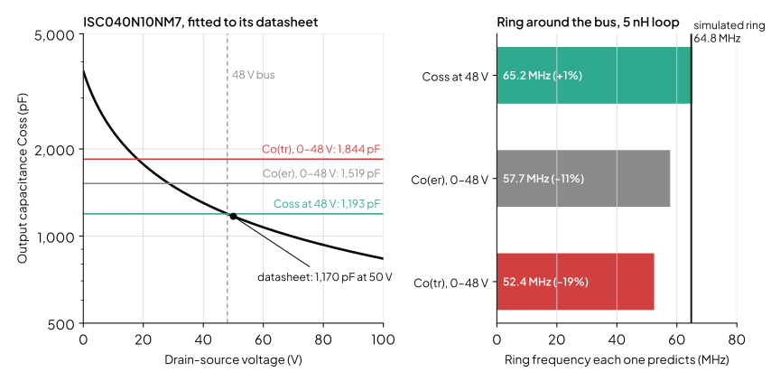
at 48 V predicts the ring to about 1%. Even a ring that swings 80% of the bus voltage stays in 1.5% of it. predicts a ring 11% too slow, and one 19% too slow. is the tempting one, because it's the "large-signal" number. It answers a different question.
So the bench and the datasheet agree when you compare the right numbers. If your bus is close to the datasheet's test voltage, the front-page figure will do. If it isn't, read the curve at your bus voltage.
If the two don't agree, a well above means extra capacitance on the node. The usual suspects are layout strays, the output inductor's winding capacitance and a Schottky diode across the low-side switch. A well below it points to the measurement: check the probe position and the frequencies you read. Output capacitance is also a selection cost in its own right, as Why the Lowest RDS(on) Isn't the Best MOSFET for Your Buck Converter explains.
Step 4 Choose the snubber capacitor
This is the real decision, and it's a trade between damping and dissipation. Define the ratio . The table uses an ideal step from 0 V to the bus through the loop inductance, with no loss and a constant . That puts the unsnubbed overshoot at 100% whatever the layout.
It isn't a bound in either direction. A slower real edge lowers the peak. The real, voltage-dependent raises it. On the fitted ISC040N10NM7 curve, the same step takes the worked example's final design to 85 V. The constant- model gives 74 V. So use the table to compare designs, and step 7 to measure yours.
For the worked example's switch and loop, with the resistor from step 5:
| Overshoot of the step | Decay time constant of the ring | Dissipation at 48 V, 500 kHz | ||
|---|---|---|---|---|
| none | — | 100% | keeps ringing | 0 |
| 0.5 | 0.60 nF | 80% | 24 ns | 0.69 W |
| 1 | 1.19 nF | 68% | 14 ns | 1.37 W |
| 1.5 | 1.79 nF | 59% | 10 ns | 2.06 W |
| 2 | 2.39 nF | 53% | 8.5 ns | 2.75 W |
| 3 | 3.58 nF | 44% | 6.5 ns | 4.12 W |
| 4 | 4.77 nF | 38% | 5.5 ns | 5.50 W |
The decay time constant is exact, from the eigenvalues of the circuit. The ring's envelope falls to 5% in about three time constants.
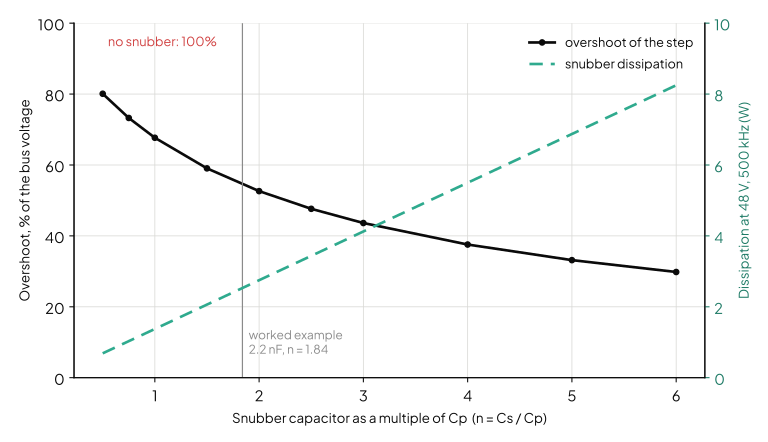
Each whole step in costs another 1.4 W. From to 2 that buys 15 points of overshoot and a ring time constant 40% shorter. From 2 to 3 it buys 9 points, and from 3 to 4 only 6. So = 2 to 3 is where the returns start to fall. Choose 2 when the watts matter and 3 when you need the margin.
The usual rules sit in this range. Todd recommends two to four times the switch capacitance, usually three [1]. TI says about three [2]. Nexperia says one to two [3].
Step 5 Choose the snubber resistor
Lan and Manenti derived the optimum resistor for an RC snubber in closed form [5]:
| 0.5 | 1 | 2 | 3 | 4 | |
|---|---|---|---|---|---|
| 2.74 | 1.73 | 1.22 | 1.05 | 0.97 |
The optimum falls as the capacitor grows, and it passes through at . That's why Todd's classic pairing of three times the capacitance with works [1].
The resistor is forgiving around that optimum. I computed the ring's decay time constant across the resistor range for four capacitor ratios:
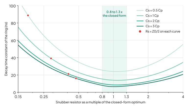
For up to 4 the closed form lands in 1% of the ring's fastest decay, and at in 7%. Anywhere from 0.8 to 1.3 times it keeps the decay in 25% of its fastest, for up to 4. So the resistor needn't be precise, and a standard value near the closed form is fine.
Avoid . It comes from setting the damping ratio of the original ring to 1 and ignores the capacitor you've just added. TI SLUA851 uses it [2], and Toshiba's note recommends anything from half to twice [6]. (Todd calls critical damping instead [1], so the phrase means different resistors in different notes.) For from 1 to 6, makes the ring decay 2.5 to 2.8 times more slowly than the optimum. It's the lingering ring that radiates.
Step 6 Check the dissipation and pick the parts
Resistor power. Use from the start of this note as the continuous rating. The resistor also takes up to as a pulse on every edge, so check its pulse rating as well. A couple of watts usually means several chip resistors in parallel, which also lowers their inductance.
Capacitor. C0G/NP0 only. Class II ceramics lose much of their capacitance under DC bias, which would move your . Rate it for at least the peak switch-node voltage.
Placement. Put the snubber at the switch's drain and source pins, with the shortest loop you can manage. Prefer thin-film resistors, which have less inductance than thick-film or leaded parts [3]. The snubber's own loop inductance, with and , forms a second, faster resonance. Nexperia shows a 146 MHz second ring on real hardware from a snubber placed away from the switch [3].
Step 7 Fit it and measure again
Fit the snubber and repeat step 1 at full load and your real bus voltage. Check three things:
- The peak is inside the switch's rating with the margin you need.
- The ring dies out in a few cycles, and no new, faster ring has appeared. If one has, it's the snubber's own loop: measure it separately and shorten that loop.
- The resistor's temperature after the board has reached thermal steady state. If it runs hotter than its derating allows, use more parallel parts or a smaller .
Worked example
A 200 W buck: 48 V bus, 500 kHz, Infineon ISC040N10NM7 as the low-side switch, 5 nH power loop. The 5 nH is a reasonably tight layout, with the input capacitor a few millimetres from the switch. The frequencies below are calculated from that assumed 5 nH and the fitted curve's at 48 V, so the calculation must return them. On a real board you'd measure them.
Before you build. The datasheet gives = 1,170 pF at 50 V, and the fitted curve gives 1,193 pF at 48 V. With 5 nH the ring should sit near 65 MHz.
- Measure. = 65.2 MHz.
- Add 3.3 nF, about 2.8 times the expected . = 33.6 MHz, so = 1.940. With each frequency read to 1% and a 1% capacitor, is good to about 6%.
- Calculate. = 3.3 nF / (1.940² − 1) = 1,193 pF, and = 5.00 nH. A 4 pF probe changes by 0.3%, so ignore it. = 2.05 Ω. On a real board, compare with the 1.19 nF expected at 48 V, as in step 3.
- Capacitor. Aim for = 2, which is 2.39 nF. Fit 2.2 nF C0G, so = 1.84.
- Resistor. The closed form gives 1.27 × 2.05 Ω = 2.60 Ω. Fit 2.7 Ω.
- Dissipation. 2.2 nF × (48 V)² × 500 kHz = 2.53 W, at most 2.53 µJ per edge. That's 1.3% of the converter's output.
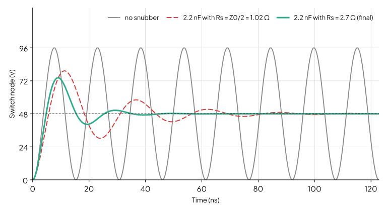
- Check. On the ideal step, the overshoot falls from 100% to 55%, and the ring decays with an 8.9 ns time constant. With instead, the overshoot would be 65% and the time constant 22.5 ns.
Assumptions and limits
- One dominant resonance. The procedure assumes the ring is one against one . A second ring from the snubber's own loop, or from another loop on the board, needs measuring on its own [3].
- Diode reverse recovery. If a diode's recovery current drives the ring, the snubber also has to absorb . Nexperia AN11160 treats this case in full [3].
- Idealised simulation. The figures come from a lossless simulation. Figs. 4 and 6 use an instant edge, and Figs. 1 and 3 a ring set up around the bus. The absolute peaks on your board depend on the edge speed, the current being switched and the real curve, which pull in opposite directions. The comparisons between designs are what the simulation is for.
- A full swing on the real curve. On the real curve, a swing from 0 V meets the large capacitance at low voltage. The overshoot is then worse than a constant- model predicts, with or without the snubber. For the resistor that minimises the peak drops to about , but the closed form's peak is only about 2 V higher. The closed form is still the right place to start, and step 7 tells you where your board sits.
If you're working from TI SLUA851
SLUA851's Eq. 4 prints two forms of the loop inductance joined by "or" [2]. The first, , is correct. The second uses the difference of the two frequencies instead of the difference of their periods squared. The two aren't equivalent, and the worked example uses the second.
Take the note's own numbers: 200 MHz, 1 nF added, 98 MHz. The correct result is = 2.00 nH and = 316 pF, not the printed 2.43 nH and 261 pF. At the note's own damping target, that makes 1.26 Ω rather than 1.53 Ω. The board was built with a 1.54 Ω resistor, so the measured waveforms in the note stand. The equation doesn't.
What this means for switchmode.io
A snubber's dissipation is already a line in switchmode.io's loss budget, next to conduction and switching loss. It belongs there, because a snubber that protects the switch still costs efficiency. That's the point of this note too. The ring is set by your layout and your switch's capacitance at the bus voltage. The capacitor is a decision about how many watts you'll spend to damp it. And the resistor has a closed-form value with a comfortable tolerance, so long as you don't halve it.
References
[1] P. C. Todd, "Snubber circuits: theory, design and application," Unitrode Power Supply Design Seminar, SLUP100, May 1993. [Online]. Available: https://www.ti.com/lit/ml/slup100/slup100.pdf (TI sign-in required)
[2] B. Gebru, "Minimizing switch ringing on TPS53318 and TPS53319 family of devices," Texas Instruments Application Report SLUA851A, Nov. 2018. [Online]. Available: https://www.ti.com/lit/pdf/slua851
[3] Nexperia, "Designing RC snubbers," Application Note AN11160, rev. 3.1, Oct. 2024. [Online]. Available: https://assets.nexperia.com/documents/application-note/AN11160.pdf
[4] M. Kasper, R. M. Burkart, G. Deboy, and J. W. Kolar, "ZVS of power MOSFETs revisited," IEEE Transactions on Power Electronics, vol. 31, no. 12, pp. 8063–8067, Dec. 2016.
[5] R. Lan and A. Manenti, "Optimizing snubber design through frequency-domain analysis," EDN, Jul. 2017. [Online]. Available: https://www.edn.com/optimizing-snubber-design-through-frequency-domain-analysis/
[6] Toshiba Electronic Devices & Storage Corporation, "RC snubbers for step-down converters," Application Note, Sep. 2018. [Online]. Available: https://toshiba.semicon-storage.com/info/docget.jsp?did=63595
[7] Infineon Technologies, "ISC040N10NM7 OptiMOS 7 power MOSFET," datasheet rev. 1.0, Nov. 2025. [Online]. Available: https://www.infineon.com/assets/row/public/documents/24/49/infineon-isc040n10nm7-datasheet-en.pdf
[8] Tektronix, "Passive voltage probes TPP1000, TPP0500B, TPP0502, TPP0250," datasheet 51W-26151-9, Oct. 2018. [Online]. Available: https://download.tek.com/datasheet/TPP1000-TPP0500B-TPP0502-TPP0250-Passive-Voltage-Probe-Datasheet-51W261519.pdf