Where it comes from, why current-mode control doesn't remove it, and how a bigger inductor can leave your loop with no valid crossover frequency at all.
Tell a boost converter to raise its output and the first thing it does is lower it. Not overshoot, not ring. It goes the wrong way for several switching cycles, then turns round and does what it was told.
A buck converter never does this, and the exemption is not an accident of the modelling. The right-half-plane zero appears in flyback, boost and Ćuk circuits and never in the buck family, and then only when they run in continuous conduction mode [1]. So if your loop design instincts were built on buck converters, they were built on the one topology that never has to deal with it.
The reason it matters is that the usual fixes make it worse. A right-half-plane zero raises the gain slope by 20dB/decade and drops the phase by 90° at the same time [2]. Cancel the gain with a pole and you add another 90° of lag. Push the crossover frequency out to get a faster response and you walk further into the phase loss. Every technique that works on a voltage-mode buck loop is the wrong tool here, because the problem is not in the compensator.
This article works through one converter. By the end there's a result worth carrying into your own designs. Two standard placement rules that every boost design uses can contradict each other, and the inductor decides which one wins. Choose it by ordinary buck reasoning and you can end up with no valid crossover frequency at all.
The design: 12V to 48V, 120W at 500kHz
The example is a 48V rail generated from a 12V input, running from 9V to 16V. It shares its input rail with the point-of-load buck used in the MOSFET selection article and the inductor sizing article. The only thing that changes here is the topology.
| Parameter | Value |
|---|---|
| 9–16V, 12V nominal | |
| 48V | |
| 120W (2.5A) | |
| 500kHz | |
| 4.7µH | |
| 100µF |
At 12V in, the duty ratio is:
So the switch is on for 1.5µs of every 2µs period, and the diode conducts for the other 0.5µs. The inductor carries the input current, which is 10A at nominal line and 13.3A at 9V. With 4.7µH the ripple is 3.83A at nominal, a ripple ratio of 0.38.
Two things matter more than anything in that table, and neither one is in it. The load resistance is = 19.2Ω, and it turns up in every loop equation below. The other is that the inductor does not behave like a 4.7µH inductor as far as the loop is concerned. That is the first surprise of the topology.
Why the output goes down when you ask it to go up
In a buck, the inductor sits between the switch node and the output. Whatever the inductor carries, the load gets. In a boost it doesn't work like that. The inductor connects to the output only through the diode, so it feeds the load only while the switch is off. Call that interval the diode conduction time, because that is the quantity the rest of this article turns on. So the DC output current is the average inductor current multiplied by , not the average inductor current itself.
That factor is where the trouble starts.
Increase the duty ratio and two things happen, on completely different timescales. The inductor current begins to rise, because there is now more volt-second product applied to it each cycle. But that takes time, since the rate is limited by . Meanwhile the diode conduction time has already fallen, in the very first cycle, because you just made the on-time longer.
Dixon set this out in 1986 and the explanation has not been improved on since [1]. The first effect lags the duty ratio by 90°. The second is immediate. Above the frequency where the inductor current can still keep up in one cycle, the second effect wins. In his words: "the output current is 180° out of phase with . This is the circuit effect which is mathematically the right-half-plane zero" [1].
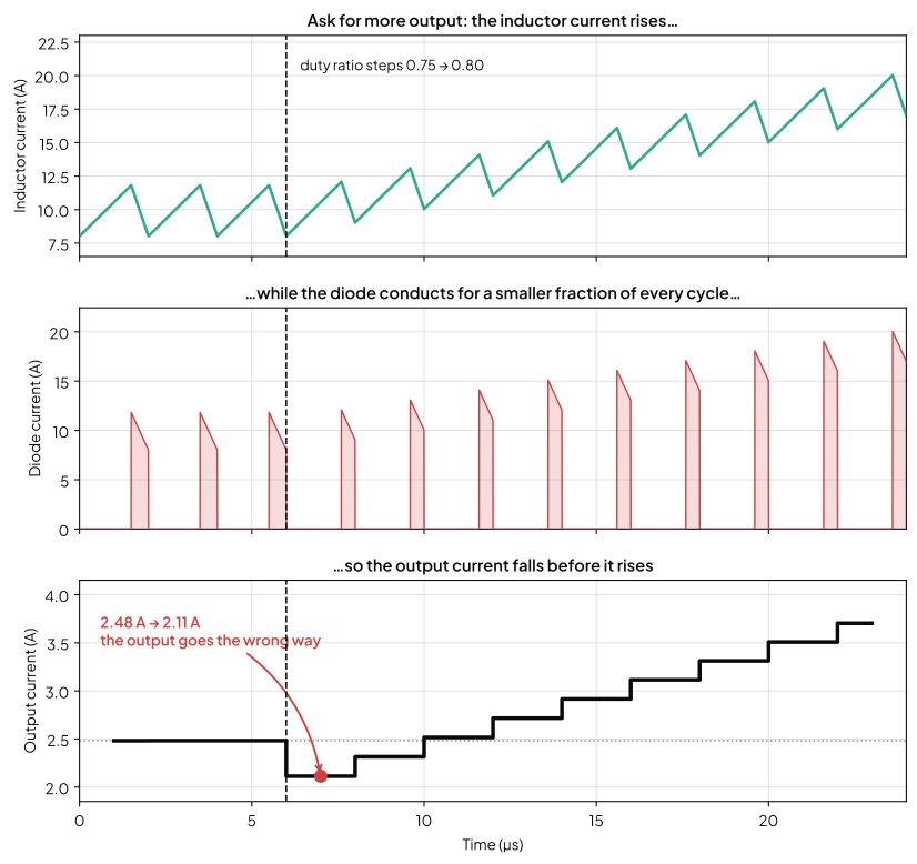
The commanded change was in the right direction. The stored energy is going up. The delivery mechanism just got worse faster than the stored energy got better.
At the output, the effect is small in absolute terms and slow to clear.
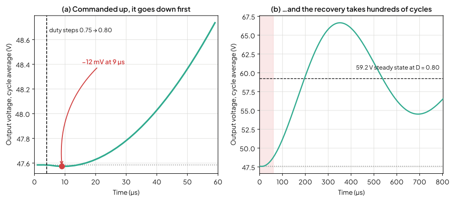
Worth being straight about the size of that dip. It is 11.6mV against 37.3mV of switching ripple, so you would not pick it out on a scope. Anyone telling you the right-half-plane zero is something you can see as a dramatic notch in the output is overselling it. The damage it does is not to this transient. It is to every transient, permanently, by capping how fast the loop is allowed to be.
What it looks like on a Bode plot
The control-to-output transfer function for a CCM boost is [2][4]:
where and the effective inductance is:
That is the second surprise. At 9V in, = 0.1875, so the 4.7µH part presents 133.7µH to the loop. The resonance sits at , which is 1376Hz, far lower than the same components would give in a buck.
The term that matters is . Note the minus sign. An ordinary zero has a plus there.
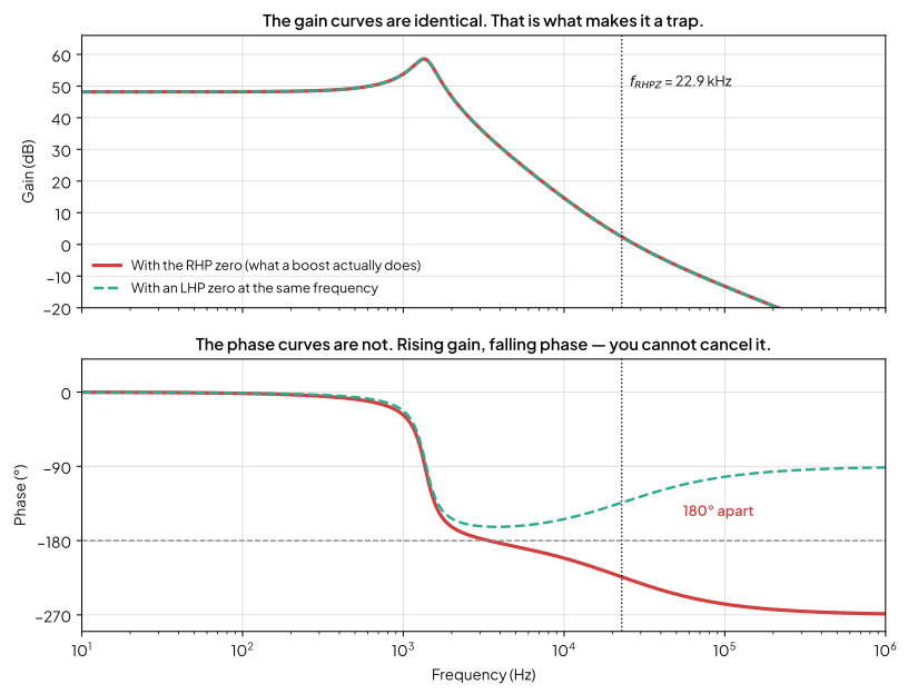
The two gain curves lie exactly on top of each other. Every gain measurement you could take says the same thing about both circuits. The phase curves separate by a full 180°, and by the time you are a decade past the zero the boost has lost 270° instead of gaining nothing.
This is why the right-half-plane zero deserves more caution than a merely awkward pole. A pole that eats your phase margin also announces itself in the gain plot, so you can see it coming and design round it. This one announces itself as good news. The gain flattens out, which normally means you have more room to push the crossover higher.
It also breaks a habit worth naming. The Bode gain-phase relationship, which lets you infer phase from the slope of the gain, only holds for minimum-phase systems. A boost in CCM is not one. If you have been reading phase off gain slopes since university, that shortcut is now wrong, and it fails in the unsafe direction.
Dixon's conclusion in 1986 was blunt, and forty years of better tools have not changed it. The right-half-plane zero "is difficult if not impossible to compensate. The designer is usually forced to roll off the loop gain at a relatively low frequency. The crossover frequency may be a decade or more below what it otherwise could be, resulting in severe impairment of dynamic response" [1].
Where the zero sits, and how far it moves
The frequency is:
That form appears in every app note [2][3], and it obscures what actually drives the answer. Substituting and gives a much more useful version:
Both give the same number. The second tells you where to look. The right-half-plane zero depends on the input voltage squared, on the output power, and on the inductance. It does not depend on the switching frequency at all, which rules out the reflex fix of switching faster.
For our converter at 12V in, = 40.6kHz. At 9V it is 22.9kHz. At 16V it is 72.2kHz.
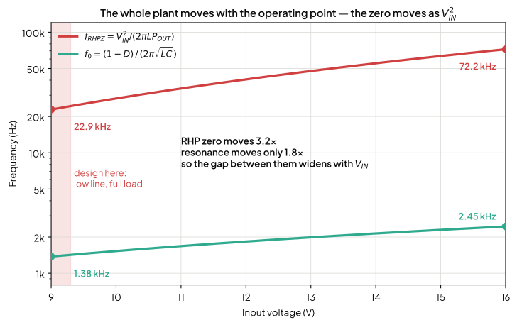
A 3.2× swing in a critical plant frequency, from nothing but the input voltage moving inside its specified range. The worst-case phase margin article looked at what ±20% component tolerance does to a buck loop. Here the operating point does considerably more damage than tolerance ever will, and it does it every time the input droops.
Both TI and Ridley give the same rule for this, and it is the right one: design at the lowest input line and the maximum load [2][3]. That corner gives the lowest right-half-plane zero and the lowest resonance together. Then check the rest of the range, because the plant you compensated at 9V is not the plant you have at 16V.
Current-mode control does not fix it
Almost every boost converter you will meet uses peak current-mode control, and there is a widespread belief that this makes the right-half-plane zero go away. It does not.
Dixon derived the current-mode case in the same 1986 paper. He works through duty-ratio control, then repeats the derivation for current-mode control. He gets the same answer both times, and says so twice. The result "is the same as Eq. 7 for duty ratio control", and "the RHP zero is clearly still present with current mode control" [1].
Which makes sense once you look back at Fig. 1. Nothing in that argument mentioned how the duty ratio got set. The diode conduction time falls whenever the on-time rises, whether a voltage-mode comparator or a current-mode comparator decided to raise it. The mechanism is in the power stage, not in the modulator.
Current mode does earn its place, just not for this. It removes the inductor pole from the outer loop, so the control-to-output response becomes first-order rather than the resonant second-order shape in Fig. 3. That is a real simplification and it is why current mode dominates in boost designs. It buys you an easier compensator. It does not buy you a faster loop.
If you are staying in voltage mode, note that a Type III compensator is not optional for a CCM boost [2]. The plant has a complex pole pair with a phase drop that a Type II cannot recover from. The Type III design article works through every component value for the buck case, and the placement arithmetic carries over unchanged.
The crossover window, and how to close it by accident
Here is the part that changes how you pick an inductor.
TI's SLVA633 gives eight rules for placing the poles and zeros of a voltage-mode boost compensator. Three of them bound the crossover frequency [2]:
- below one fifth of the right-half-plane zero frequency
- above twice the power-stage resonance
- below one tenth of the switching frequency
The first is the familiar one. Ridley gives the same one-fifth figure [3], and Dixon's "a decade or more" is more conservative still [1]. The second gets much less attention. It is there because crossing over below the resonance means closing the loop through a 180° phase drop you have not passed yet.
Now watch what those two do as the inductor changes. The right-half-plane zero goes as . The resonance goes as , because . So as you increase the inductance, the ceiling falls twice as fast as the floor rises, on log axes. The window between them narrows from both sides.
Past some inductance it shuts completely. Setting and solving for :
To be clear about where that comes from: it is an algebraic consequence of combining two of TI's rules, not a result TI states. Treat the two rules as the rules of thumb they are, and the window narrows continuously rather than slamming shut at a bright line. The behaviour is real either way.
For our converter at low line, that lands at 12.96µH.
| Ripple ratio | Ceiling | Floor | Window | ||
|---|---|---|---|---|---|
| 2.2µH | 0.499 | 48.8kHz | 9.77kHz | 4.02kHz | open |
| 3.3µH | 0.332 | 32.6kHz | 6.51kHz | 3.29kHz | open |
| 4.7µH | 0.233 | 22.9kHz | 4.57kHz | 2.75kHz | open |
| 6.8µH | 0.161 | 15.8kHz | 3.16kHz | 2.29kHz | open |
| 10µH | 0.110 | 10.7kHz | 2.15kHz | 1.89kHz | open, barely |
| 12.96µH | 0.085 | 8.29kHz | 1.66kHz | 1.66kHz | shut |
| 15µH | 0.073 | 7.16kHz | 1.43kHz | 1.54kHz | no solution |
| 22µH | 0.050 | 4.88kHz | 977Hz | 1.27kHz | no solution |
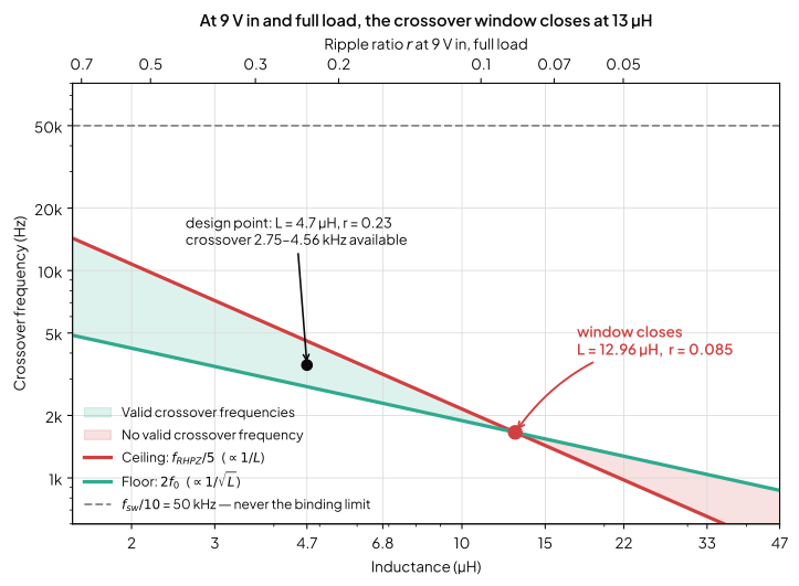
Read the ripple ratio column, because that is the whole point.
The window closes at = 0.085. That is a smooth, quiet, low-ripple inductor, and it is the kind of part you would pick for an easy life on core loss and EMI. In a buck it would be a slightly conservative choice and nothing worse. Here it means no compensator satisfies the design rules. No amount of care with the Type III arithmetic will produce one, because there is no target crossover frequency left to aim at.
The buck inductor article argues for a ripple ratio between 0.25 and 0.5, and shows the loss optimum is a broad basin rather than a point. That is correct, and it is correct for a buck. It is not enough here. The boost puts a second constraint on , and it has nothing to do with loss, size or saturation. That constraint has a hard upper bound. The buck's only has a preference.
Notice also which limit never binds. One tenth of the switching frequency is 50kHz, and it sits above everything else in Fig. 5 by a wide margin. At 500kHz, the switching frequency is not what is holding your crossover frequency down. Raising it would not help.
What to actually do about it
Reduce the inductance. It is the only lever in that you fully control, and it moves the zero proportionally. This runs directly against the instinct to smooth out ripple, and in a boost the instinct is wrong.
TI gives a number for this, and it is worth reading carefully. Their guidance is an inductor "where the peak-to-peak ripple current in the inductor at full load is about 50% of the dc output current of the converter" [2]. In a buck those are the same current. In a boost they differ by a factor of , which here is 5.3, so the sentence has two readings that are a long way apart:
- 50% of the output current (2.5A) means 1.25A of ripple, which is 11.7µH at low line.
- 50% of the inductor's own DC current (13.3A) means 6.67A of ripple, which is 2.2µH.
Take the second. The first sits within 10% of the 12.96µH where the crossover window shuts, which cannot be what a controllability rule is aiming at. Resolve it explicitly rather than reaching for the number you would have used on a buck. This particular ambiguity only bites on the topology where it matters most.
Accept the crossover frequency you are given, and solve the transient problem with the output capacitor instead. With capped near 4.5kHz at low line, the loop cannot respond to a load step for the first couple of hundred microseconds. Whatever charge the load takes in that window comes out of the output capacitor. Size it for that, not for ripple.
Design at low line and full load, then verify across the range. Both TI and Ridley are explicit about this [2][3], and Fig. 4 shows why. The plant moves further with operating point than with anything on your tolerance stack.
Raise the input voltage if the system architecture gives you any say. The zero goes as , so a 12V bus instead of a 9V one nearly doubles it. This is usually someone else's decision, which is exactly why it is worth raising early rather than discovering the constraint after the architecture is fixed.
Two things that sound like fixes and are not. Discontinuous conduction mode does simplify the control problem, because the LC filter is heavily damped and the response becomes essentially first-order. But SLVA633 says plainly that DCM "is not necessarily recommended as a solution to control problems". Higher-power boost converters are designed for CCM on efficiency grounds [2]. There is also a real literature on eliminating the right-half-plane zero through coupled magnetics or tri-state switching. Those are topology changes rather than compensation, and they are not advice for someone building a conventional boost.
Where this leaves you
The right-half-plane zero is not a modelling artefact and it is not a control problem. It is the converter behaving exactly as the circuit requires, and the loop inheriting the consequence.
What makes it worth an article is the coupling it creates. In a buck you can choose the inductor for ripple, loss and size, then design the loop around whatever you chose. In a boost that separation doesn't hold.
The inductor sets the right-half-plane zero. The zero caps the crossover frequency. The crossover frequency sets how much charge the output capacitor has to supply on a load step. And the capacitor moves the resonance, which is what sets the lower bound on crossover in the first place. Pick the inductor last and you may find the loop has already been decided for you. Pick it first, on buck instincts, and Fig. 5 is what can happen.
Holding all of those constraints at once, at the operating corner where each is worst, with real part data rather than typical values, is exactly the analysis switchmode.io is being built to do. Four separate calculators cannot tell you that the inductor you picked closed your crossover window, because none of them knows what the others chose.
References
[1] L. H. Dixon, Jr., "The Right-Half-Plane Zero — A Simplified Explanation," Unitrode Power Supply Design Seminar SEM500, Topic C2, 1986. Reproduced by Texas Instruments, SLUP084. [Online]. Available: https://www.ti.com/seclit/ml/slup084/slup084.pdf
[2] S. W. Lee, "Practical Feedback Loop Analysis for Voltage-Mode Boost Converter," Texas Instruments Application Report SLVA633, January 2014. [Online]. Available: https://www.ti.com/lit/pdf/slva633
[3] R. Ridley, "[017] Boost Converter with Voltage-Mode Control," Ridley Engineering Design Center. [Online]. Available: https://ridleyengineering.com/design-center-ridley-engineering/38-control/60-017-boost-converter-with-voltage-mode-control.html
[4] R. W. Erickson and D. Maksimović, Fundamentals of Power Electronics, 3rd ed., Springer, 2020.