An undamped input filter resonates, and a regulating converter looks like a negative resistance at its input. Put the two together and the bus oscillates. The fix is a damping resistor in series with a blocking capacitor , connected across the filter capacitor. This note starts from a filter that already exists. It finds the smallest and that hold the filter's output impedance under a stated limit, and the power rating the resistor needs.
Three things here aren't in the usual references. The published design procedures run forwards, from a damping capacitor you picked to the impedance you got. This note inverts them and picks the capacitor from the impedance you need. Three separate references say the blocking capacitor is there to avoid dissipation in the resistor, and none of them says how much is left. This note bounds it in one line. And the resistor turns out to be the loose tolerance and the capacitor the tight one. That's the opposite of how the usual rule of thumb is applied.
This note sizes the damping for a filter you already have. Choosing the filter itself is the other half, and Input Filter Design: The Inductor Sets Your Stability Margin does that.
Before you start: do you need a damping network?
A real filter is never undamped. The inductor's DC resistance and the capacitor's equivalent series resistance (ESR) already damp it, and sometimes they damp it enough. Check that first:
where:
- is the quality factor of the filter with no damping network fitted.
- is the peak of the filter's output impedance . That's the impedance the converter sees looking back into the filter, with the source shorted.
- is the filter's characteristic impedance, from step 1.
- is the filter inductance, and is the filter capacitance at the bus voltage.
- is the filter inductor's DC resistance.
- is the filter capacitor's ESR.
That estimate is good to better than 2% for any above 5, and better than 0.5% above 10. If is already under the limit from step 2, fit nothing.
It rarely is. In the worked example, a 25 mΩ inductor and a 3 mΩ ceramic leave = 73. That's a 149 Ω peak against a limit of 5.77 Ω.
Two other fixes come before a damping network, and both are free. A more resistive inductor damps the filter at no component cost, though it costs efficiency in the DC current. A different split of the same product changes directly, and the peak scales with it. If step 3 asks for a damping capacitor you can't fit, that split is what to change.
What you need
- and , with taken at the bus voltage, not from the label. A class II ceramic loses a large part of its capacitance under DC bias. The example's 4.7 µF 100 V X7R is 2.4 µF at 48 V.
- The inductor's DC resistance and the capacitor's ESR, for the check above.
- The converter's input power and its minimum bus voltage. Both set the impedance you have to stay under.
- The margin you're designing to, in dB. 6 dB is the usual figure in aerospace and military work [7].
- The AC ripple voltage across the filter capacitor, measured or calculated. Step 5 needs it.
- The ESR of the damping capacitor, if you plan to use an electrolytic. It's part of .
Step 1 Characteristic impedance and corner frequency
where:
- is the filter's characteristic impedance.
- is its resonant frequency, which is also its corner frequency.
- is the filter inductance.
- is the filter capacitance at the bus voltage, not the value on the label.
Everything that follows is normalised to .
Step 2 The peak you're allowed
Inside its control bandwidth a converter holds its input power constant, so its incremental input resistance is negative:
where is the converter's incremental input resistance, is its input voltage, and is its input power. is the output power divided by the efficiency.
Middlebrook's criterion says the filter's output impedance has to stay well below that magnitude at every frequency [6]. With a margin, the filter's peak output impedance must stay under
where is the largest peak output impedance the filter is allowed, is the magnitude of , and is the margin in dB.
At 6 dB the divisor is 1.995, not 2. Evaluate at the minimum bus voltage, which is where it's smallest. If the bus has a wide range, run steps 1 to 4 at both ends. falls as the bus rises, and that pushes the other way.
What "well below" should mean is a longer argument than this note. Middlebrook Stability Criterion: Why Failing It Doesn't Mean Your Converter Is Unstable works through seven criteria that answer it.
Step 3 The damping capacitor
Define , the ratio of the damping capacitance to the filter capacitance. With the damping resistor at its optimum for that , the peak output impedance is [1], [2]:
where is the filter's peak output impedance, is its characteristic impedance from step 1, and is the capacitance ratio.
Every published procedure uses that forwards. You choose , usually 4 because that's the rule of thumb, and find out what peak you got. Run it the other way instead. Write , which is the allowed peak from step 2 as a multiple of . Set equal to , square both sides, and it's a quadratic in :
Take the positive root, because can't be negative:
where:
- is the smallest capacitance ratio that reaches the allowed peak.
- is that peak as a multiple of .
- is the filter capacitance at the bus voltage.
- is the damping capacitance needed. It charges to the full bus voltage as well, so it's also a value at bias.
That's the smallest damping capacitor that can reach the target, and it's exact.
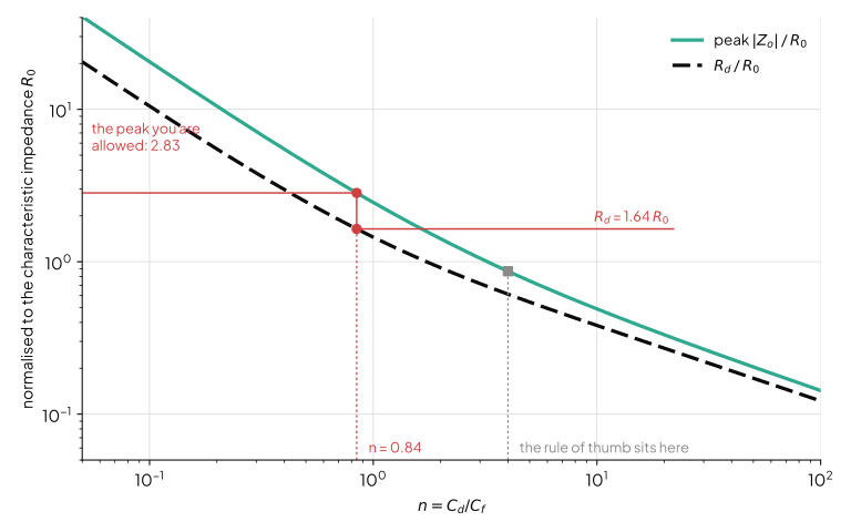
Two sanity checks on the result. For small , meaning you're a long way above the target, . The damping capacitor grows as the square of how far you have to come down. At = 0.1 the exact answer is 202 and gives 200. For large , , and the capacitor becomes small.
If comes out above about 10, stop. A damping capacitor ten times the filter capacitor means the filter is badly split, and resizing and is cheaper than buying the electrolytic. Part 2 covers that.
Step 4 The damping resistor
For the you just found, the resistance that minimises the peak is [1], [2], [3]:
where is the total series resistance of the damping branch, is the characteristic impedance from step 1, and is from step 3.
Subtract the damping capacitor's ESR from that number, because the ESR is in series with the resistor and does the same job. With a ceramic the ESR is a few milliohms and you can ignore it. With an aluminium electrolytic it can be most of , or more than all of it. Then that capacitor can't reach the optimum, however small a resistor you fit next to it. The other way round, an electrolytic whose ESR lands near needs no resistor at all.
The peak lands at
where is the frequency of the peak output impedance, is the resonant frequency from step 1, and is the capacitance ratio. is below , and it moves further below it as grows. Measure there.
is not the optimum. It's the common rule of thumb, and it's only right near = 1.73. At = 4 the optimum is 0.61 , and at = 0.84 it's 1.64 .
Nothing here costs you attenuation. At high frequency the branch looks like in parallel with . That's a lower impedance than alone, so the filter attenuates marginally more than it did. In the worked example, 47.45 dB becomes 47.48 dB. The two alternatives use a damping inductor instead of . A resistor and inductor in series, across the filter inductor, costs high-frequency attenuation by a factor of . Here is the damping inductance over . The other puts a resistor in series with the filter inductor, with an inductor across it to carry the DC. It can't get the peak below with any inductor [1]. Those are the reasons to prefer this network.
Step 5 What the resistor dissipates
Erickson [1], Sclocchi [3] and TI SNVA801 [4] all say the blocking capacitor is there to avoid dissipation in . None of them says how much is left. It isn't zero. blocks the DC, and the converter's ripple current goes straight through it.
The damping branch sees the ripple voltage across the filter capacitor. Each harmonic of that ripple drives a current of through the branch, so
where:
- is the average power dissipated in the damping resistor.
- is the harmonic number of the switching frequency: 1, 2, 3 and so on.
- is the rms ripple voltage across at harmonic .
- is the angular frequency of harmonic , and is the switching frequency.
- and are the damping resistance and capacitance from steps 3 and 4.
- is the total rms ripple voltage across , without its DC level, which blocks.
The bound is one line, always true, and tight wherever the ripple sits well above the damping branch's own corner frequency, . That is normally all of it. In the worked example the bound is 0.2% above the harmonic sum. Use the bound.
You can put a scope on . If the board doesn't exist yet, the fundamental carries most of it. For a buck:
where:
- is the rms value of the fundamental of the converter's input current.
- is the buck's output current.
- is its duty cycle.
- is the switching frequency.
- is the filter capacitance at the bus voltage.
- is the total rms ripple voltage across .
The first form treats the input current as rectangular pulses of height , which ignores the inductor's current ripple. The second takes all of that current into .
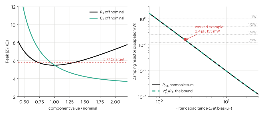
The dissipation depends almost entirely on the filter capacitor. That's worth knowing before you pick a package, because the answer ranges over three orders of magnitude across filters that all meet the same criterion.
Step 6 Put the margin on the capacitor, not the resistor
The optimum in step 4 is flat and the constraint in step 3 is a cliff. Fig. 2 shows both. Halving or doubling it costs about 2 dB. Losing 20% of costs 1.3 dB, and losing 40% costs 4.0 dB.
That asymmetry decides where the tolerance goes. Size from the worst-case , meaning after tolerance, DC bias and end of life, and then let the resistor be a standard value. In the worked example, allowing both capacitors to run 20% low moves from 0.84 to 0.96 and from 3.35 Ω to 3.40 Ω. The capacitor has to grow by 14%. The resistor barely moves.
It also explains why = 4 has survived as a rule of thumb. It's over-specified for most targets, and being over-specified is what makes it insensitive.
Step 7 Check it
- Sweep or simulate with the source shorted, and confirm the peak and its frequency. Include the DC resistance and the ESR. They only help.
- Confirm the attenuation at the switching frequency hasn't moved.
- Measure the ripple across on the built board and redo step 5 with the real number.
- Check the resistor's temperature at full load, after the board has reached steady state.
Worked example
A 200 W buck: 48 V bus, 12 V at 16 A, 500 kHz, 96% efficient. The filter is already on the board. The inductor is 10 µH with 25 mΩ of DC resistance. The capacitor is a 4.7 µF 100 V X7R with 3 mΩ of ESR, and its bias curve gives 2.4 µF at 48 V.
- Characteristic impedance. = 2.04 Ω, and = 32.5 kHz. The filter gives 47.5 dB at 500 kHz. Undamped, = 149 Ω, so it needs damping.
- The peak allowed. = 200 W, so = 11.52 Ω. At 6 dB, = 5.77 Ω.
- The capacitor. = 5.77/2.04 = 2.83, so = 0.84, and = 2.02 µF at bias.
- The resistor. 1.64 × 2.04 Ω = 3.35 Ω. The peak will sit at 27.3 kHz.
- Dissipation. = 5.09 A at 500 kHz, which puts 0.68 V rms across . Summing the harmonics gives 0.72 V, so = 0.16 W.
- Tolerance. Allow 20% low on both capacitors and has to be 2.31 µF nominal at bias.
- What to fit. A second 4.7 µF 100 V X7R, identical to the filter capacitor, gives 2.4 µF at bias and = 1.00 exactly. Its optimum resistor is 2.96 Ω, so fit 3.0 Ω. That's 0.17 W, so a half-watt chip.
The result peaks at 4.78 Ω at 26.7 kHz, which is 7.6 dB below the converter's input impedance against the 6 dB asked for.
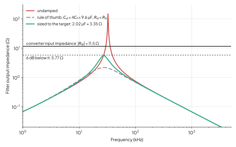
The rule of thumb isn't wrong here. It's expensive. It reaches 2.17 Ω when 5.77 Ω would have done. On a 48 V bus, that extra 7.6 µF is a part you have to find room and voltage rating for. It's also not at its own optimum: with the right resistor for = 4, the same 9.6 µF would reach 1.72 Ω.
If you're working from Power Tip #4
Kollman's chart [5] is the only published way to run the design backwards, and it's the method this note replaces with an equation. Its worked example doesn't hold up, so check anything you read off it.
The example takes a 10 µH and 10 µF filter, so = 1 Ω, feeding a 12 W supply at 12 V. That allows a 6 Ω peak, and the chart is entered at = 6. In this note's symbols, the article reads off = 0.1, so 1 µF, and = 3, so 3 Ω. (Kollman writes them as and .) That network peaks at 39.4 Ω, 16 dB above the target.
The two values are inconsistent with each other, which points at the reading rather than the chart. The resistor is right: the exact optimum for a 6 Ω peak is 3.24 Ω. The capacitor isn't, and = 0.1 can't reach 6 Ω with any resistor at all, because its own best is 20.5 Ω. The correct answer is = 0.362, so 3.62 µF and 3.24 Ω, which the equation in step 3 returns directly.
Assumptions and limits
- One filter section, and a stiff source. The output impedance is taken with the source shorted. A second section in front changes it, and Erickson gives the conditions under which it doesn't [1]. Cascaded stages and distribution buses behave differently again, which Middlebrook's Criterion in Practice covers.
- A constant-power load. holds inside the converter's control bandwidth. Above it the converter's input impedance rises towards its open-loop value, and the criterion gets easier. If the filter resonance sits near or above the crossover frequency, this note is conservative.
- The magnitude-only criterion. Keeping a fixed number of dB below the converter's input impedance is sufficient, not necessary. A design that fails it can still be stable, and part 1 shows by how much.
- Ripple modelled as a rectangular pulse train. Step 5 ignores the inductor's current ripple, which makes the harmonics slightly pessimistic. It also ignores any capacitance local to the converter, which takes ripple that would otherwise reach the filter node. Both errors are in the safe direction. Measure the ripple on the built board.
- Steady state only. The dissipation figure covers the switching ripple. A bus step or a large load step rings the filter, and absorbs that energy too. On a repetitively pulsed load, check the resistor's pulse rating as well as its continuous rating.
- assumed resistive at . True for any sensible chip resistor at tens of kilohertz.
What this means for switchmode.io
An impedance margin is a number, and it should be an input to the design rather than something you discover afterwards. That's the whole argument for sizing the damping network from the margin instead of a rule of thumb. It's also the argument switchmode.io is being built around. The input filter calculator takes the rail, the switching frequency and an attenuation target. It sizes the filter and its damping network, and reports the Middlebrook and GMPM margins it achieved. It has a check mode for a filter you already have, which is the case this note is written for.
References
[1] R. W. Erickson, "Optimal single resistor damping of input filters," in Proc. IEEE Applied Power Electronics Conf. (APEC), 1999, pp. 1073–1079.
[2] R. W. Erickson and D. Maksimović, Fundamentals of Power Electronics, 3rd ed. Springer, 2020, ch. 17.
[3] M. Sclocchi, "Input filter design for switching power supplies," National Semiconductor / Texas Instruments SNVA538, 2010. [Online]. Available: https://www.ti.com/lit/an/snva538/snva538.pdf
[4] Texas Instruments, "Analysis and design of input filter for DC-DC circuit," Application Report SNVA801, Nov. 2017. [Online]. Available: https://www.ti.com/lit/an/snva801/snva801.pdf
[5] R. Kollman, "Power Tip #4: Damping an input filter, part 2 of 2," EDN, Sep. 29, 2008. [Online]. Available: https://www.edn.com/power-tip-4-damping-an-input-filter-part-2-of-2/
[6] R. D. Middlebrook, "Input filter considerations in design and application of switching regulators," in Proc. IEEE Ind. Appl. Soc. Annu. Meeting, 1976, pp. 366–382. [Online]. Available: https://ridleyengineering.com/images/pdf/Middlebrook1976BritishLibrary.pdf
[7] SynQor, "Input system instability," Application Note Doc# 065-0000060. [Online]. Available: https://www.synqor.com/document-download?document=Input+System+Instability.pdf