Two converters can each be unconditionally stable on the bench and then oscillate the moment you connect them together. The mechanism behind this, impedance interaction at the interface, was formalised by R. D. Middlebrook in 1976 for the input-filter case [1]. But the same criterion applies wherever regulated stages share an interface. This includes cascaded converters and distribution buses feeding many point-of-load regulators.
This article works through Middlebrook's criterion with a concrete numerical example for each of those three scenarios, showing what the source output impedance and load input impedance actually look like, where they collide, and how to fix each case. If you want a broader comparison of interface stability techniques (GMPM, opposing argument, ESAC and friends), see Part 1 of our input filter stability series. If you want to size a filter rather than test one, Part 2 covers that. Here we stay on Middlebrook and how to apply it.
The core idea: minor loop gain
Take any interface in a power system and split it into a source subsystem (everything upstream, characterised by its output impedance ) and a load subsystem (everything downstream, characterised by its input impedance ). Fig. 1 shows the arrangement.
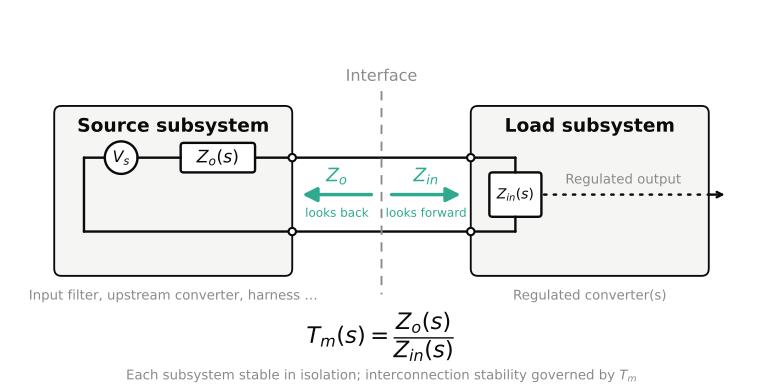
If each subsystem is stable on its own, the interconnected system's stability is governed entirely by the minor loop gain:
The interconnection is stable if and only if satisfies the Nyquist criterion: no encirclements of . Loading one stable system with another inserts into the transfer functions at the interface, and that term is where the trouble lives.
Why a regulated converter fights back
The reason this matters at all is that a regulated converter does not look like a resistor from its input terminals. Within its control bandwidth it holds output power constant, so if the input voltage dips, the input current rises. Differentiate and you get an incremental input resistance of:
Negative. A converter drawing 30W from a 24V rail presents roughly to whatever feeds it. That negative resistance can undamp any resonance it sees looking back into the source, whether that's an input filter or an upstream converter's output stage, and turn a well-behaved LC into an oscillator.
Middlebrook's answer
Middlebrook's original criterion sidesteps the Nyquist plot entirely: if
then everywhere, can never reach regardless of phase, and stability is guaranteed unconditionally. In practice "much less than" becomes a design margin, commonly 6 dB, i.e. . On the complex plane this confines to a disc around the origin; everything outside that disc is the forbidden region (Fig. 2).
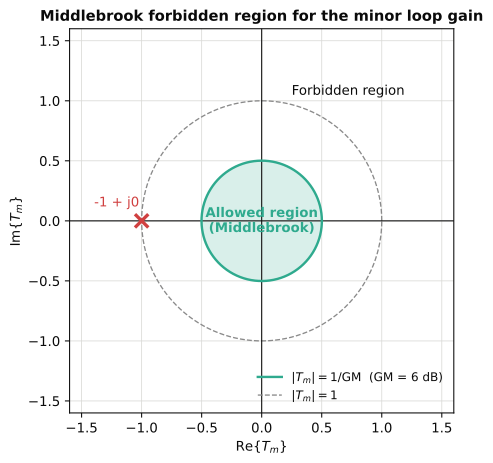
The criterion needs only magnitude information (two impedance plots on the same axes) and it makes the fix obvious: push down, or push the impedances apart in frequency. Its known weakness is conservatism. It prohibits many perfectly stable designs because it ignores phase entirely, and less conservative criteria such as Gain Margin–Phase Margin (GMPM) shrink the forbidden region to a wedge around the point. Those are worth knowing when a Middlebrook-compliant design would be prohibitively expensive. For the majority of designs, though, meeting Middlebrook with 6 dB margin is cheap and needs no phase measurement, and the margin holds up as component values drift with temperature and tolerance. That's the approach I take in all three scenarios below.
The input filter: the classic case
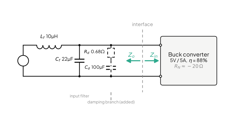
This is the problem Middlebrook originally solved. A 24V rail feeds a 5V / 5A buck through an EMI filter (Fig. 3). At 88% efficiency, W, so:
The filter is a single LC stage: (DCR 10mΩ), ceramic (ESR 3mΩ).
The source side: filter output impedance
Looking back into the filter from the converter's input terminals, is the inductor branch in parallel with the capacitor branch. It peaks at the filter resonance:
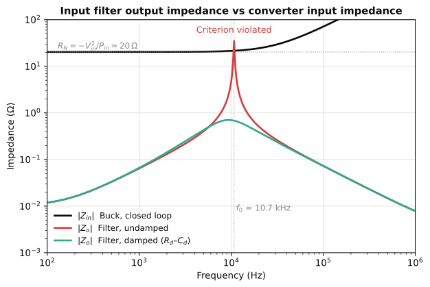
A characteristic impedance of 0.67Ω sounds harmless next to a 20Ω load, until you account for the Q. With only 13mΩ of total series resistance, , and the impedance peak reaches 35Ω. Ceramic capacitors are the villain here: their near-zero ESR is exactly what you want for ripple and exactly what you don't want for damping.
The load side: converter input impedance
Within its loop bandwidth the buck presents . Above the bandwidth the loop stops defending constant power and the input impedance transitions towards the open-loop input impedance of the power stage. For a buck this is dominated by the inductor reflected through the duty ratio, . A useful first-order model for plotting is : flat at , then rising inductively. (For the full derivation of closed-loop input impedance, TI's SLVA662 is a good reference [2].)
The collision
Fig. 4 overlays the curves. The undamped filter peak at 10.7 kHz punches straight through the converter's : a clear criterion violation.
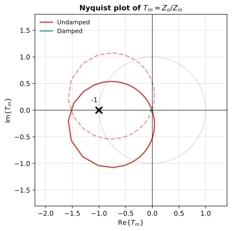
The Nyquist plot of (Fig. 5) confirms it: the undamped locus swings out past .
The fix: a damping snubber
The remedy is a damping network, an RC or RL snubber placed across one of the filter elements. (Not to be confused with the switch-node RC snubber inside the converter, which tames ringing on switching parasitics and does nothing for interface stability.) There are three standard placements [3], and the choice is a genuine trade-off rather than a matter of taste.
Option 1: – across the filter capacitor. The most common choice and my default. The design rules of thumb:
- . The damping capacitor must dominate at resonance so that actually appears across the tank. Here: 100µF.
- then follows from that choice, and it isn't . With , the resistance that minimises the impedance peak is , and the peak it achieves is [3]. At = 4.5 the optimum is . Here: 0.39Ω. You will often see given as the rule of thumb. It is within a tenth of a dB at = 2, but it gives away 2.6 dB by = 4.5 and 5.3 dB by = 8. The larger the damping capacitor, the more the rule of thumb costs you.
No DC current flows through the branch, so dissipates almost nothing. The cost is bulk: a capacitor four times the size of the one you already have. A convenient practical trick is that an aluminium electrolytic of the right value often supplies both and in one part, its ESR doing the damping. Check the ESR across temperature, though; it can triple at −40°C, and I'll come back to why that matters in the cascaded case. With the branch fitted, the peak drops from 35Ω to 0.52Ω (Fig. 4), and the Nyquist locus collapses to a small loop near the origin (Fig. 5).
Option 2: directly across the filter inductor. One resistor, no added capacitance. Attractive where bulk capacitance is constrained, by inrush limits or hot-swap requirements for example. The price is steep and often overlooked: above resonance, the noise current path runs through instead of being blocked by , and the filter's attenuation slope degrades from −40 dB/decade to −20 dB/decade. In our example, an of 1.0Ω holds the peak to 0.97Ω but gives up 30 dB of attenuation at 500 kHz (Fig. 6). If the filter exists to pass a conducted emissions limit, that 30 dB was the whole point of fitting it.
Option 3: – in series, across the filter inductor. The blocking inductor restores the DC and high-frequency isolation that Option 2 gives away: at high frequency the parallel combination is still inductive (), so the −40 dB/decade slope survives, only shifted up slightly. With and , the peak sits at 1.6Ω and the 500 kHz attenuation is within 6 dB of Option 1. The cost is a second inductor, which usually makes this the loser on price and board area against Option 1 unless capacitor volume is the binding constraint.
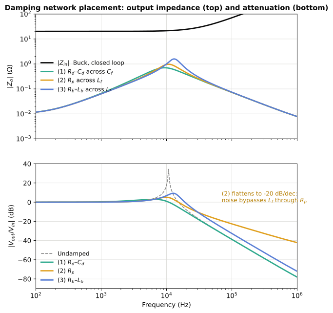
| Placement | Peak (this example) | Attenuation at 500 kHz | Cost | |---|---|---|---| | (1) – across | 0.52Ω | −67 dB | Bulk capacitance () | | (2) across | 0.97Ω | −37 dB | One resistor; wrecks HF attenuation | | (3) – across | 1.59Ω | −61 dB | Second inductor |
My ranking: Option 1 unless capacitance is genuinely constrained, then Option 3. Option 2 only where the filter isn't doing EMC duty, which in my experience is rare enough that I treat it as a last resort.
Cascaded stages: when the source is another converter
Now replace the passive filter with an active source: a 48V-to-12V voltage-mode bus converter feeding a 12V-to-1.0V / 20A point-of-load (POL) regulator (Fig. 7). Same criterion, but the character of changes completely.
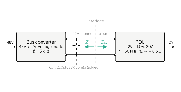
The example system:
- Bus converter: , (ESR 20mΩ), voltage-mode control, crossover = 5 kHz.
- POL: 20W output at 90% efficiency, so W and ; crossover 30 kHz.
Where an active source's output impedance peaks
Below its crossover, the bus converter's feedback loop suppresses its output impedance: , and is large. Above crossover, the loop is gone and reverts to the passive output filter. The danger zone is the crossover region itself, where two effects conspire. Loop gain has fallen to unity so suppression is nearly finished, and in a voltage-mode design with modest phase margin, actually dips below one, amplifying the open-loop impedance rather than suppressing it.
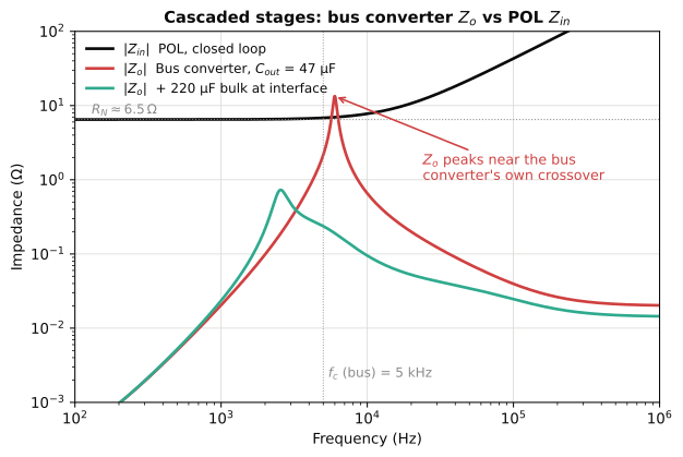
In this example it's worse still, because the output filter resonance ( kHz) lands almost on top of the 5 kHz crossover. The closed-loop peaks at 13Ω at 6 kHz, twice the POL's 6.5Ω input impedance magnitude. Violation.
Note the contrast with the input-filter case: there the peak sat at a passive resonance you chose when you picked L and C; here it sits at the source converter's crossover, a frequency set by its compensation. This is why the common rule of thumb of separating the bandwidths of cascaded stages helps but is not sufficient on its own. Our POL crossover (30 kHz) is six times the bus converter's (5 kHz), and the system still fails, because the POL's negative-resistance region extends right down through the bus converter's crossover. Bandwidth separation controls where the interaction happens; it doesn't remove it.
The fix: damped intermediate bus capacitance
Adding bulk capacitance at the interface, electrically part of the bus converter's output, reshapes in two ways. It pulls the output filter resonance below crossover, where the loop still has gain to suppress it, and its series resistance damps what remains. Here, a 220µF bulk capacitor with 50mΩ ESR drops the peak from 13Ω to 0.7Ω (Fig. 8).
Be clear about what's doing the work: this is the same – snubber as Option 1 above, with the capacitor's own ESR playing . That framing exposes the weak point. ESR is not a controlled parameter. A typical aluminium electrolytic's ESR varies 3:1 or more from 25°C to −40°C and rises further as the part ages and dries out, so a design that has exactly enough damping at room temperature can be marginal at cold start in year five. And the failure can go the other way too: a well-meaning BOM substitution to an ultra-low-ESR polymer part removes the damping resistance entirely and leaves a residual peak the original design never had.
Where the design has to hold over a wide temperature range, or survive uncontrolled substitutions, fit the snubber deliberately: a low-ESR capacitor in series with a discrete damping resistor whose value you chose and toleranced, rather than a datasheet ESR you hoped for. The resistor costs pennies and turns the damping from an accident of construction into a design parameter. Whichever route you take, note the value in the schematic as a damping element so nobody "improves" it later.
One more caution: adding capacitance at its input changes the POL's own loop plant slightly. Re-check the POL's phase margin after the change, particularly if it senses input voltage for feedforward.
The distribution bus: one source, N loads
The distribution bus is where Middlebrook analysis most often gets skipped, and where the most counterintuitive failure lives: every source–load pair can pass the criterion individually while the aggregate system fails.
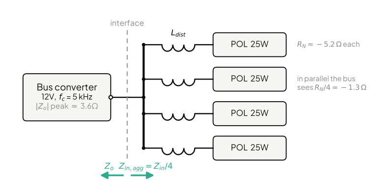
The example system: a 12V bus converter (, , ESR 25mΩ, = 5 kHz) feeds four identical 25W POLs at 90% efficiency.
Admittances add
Each POL presents:
But input admittances in parallel add, so the bus sees:
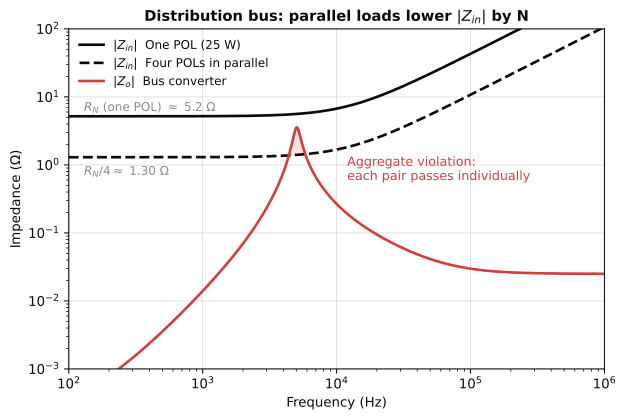
The bus converter's closed-loop peaks at about 3.6Ω near its 5 kHz crossover. Against a single POL: 3.6Ω < 5.2Ω. Passes, with a little margin even. Against four: 3.6Ω > 1.3Ω, a broadband violation spanning nearly a decade (Fig. 10). A system integrator checking each rail-to-load pair in isolation would sign this off; the first full-system power-up would say otherwise.
Distribution parasitics make it worse
The wiring between source and loads is not free. Each nH of trace or harness inductance between the bus converter's output capacitors and a POL's input adds series impedance to the that particular load sees, raising the source impedance at exactly the frequencies where the margin is thinnest and decoupling that load from the bulk capacitance that was supposed to protect it. On a compact PCB this is a dB or two; over a wiring harness it can dominate. The criterion must be evaluated at each load's terminals, with the interconnect impedance included on the source side.
Design approach: budget the admittance
For a bus, the clean method is to treat the criterion as an admittance budget:
- Characterise (or specify) the bus converter's including bulk capacitance and worst-case interconnect. If the damping relies on capacitor ESR, use the cold-temperature ESR here, for the reasons argued above.
- Set the total allowed load admittance from the margin target: for 6 dB.
- Allocate that budget across loads, in proportion to power, since at low frequency.
- Any new load added later must fit within the remaining budget, or the bus capacitance must grow to compensate.
That last point is the practical payoff: it turns "will adding this card destabilise the bus?" from a re-analysis exercise into a line item on an interface spec.
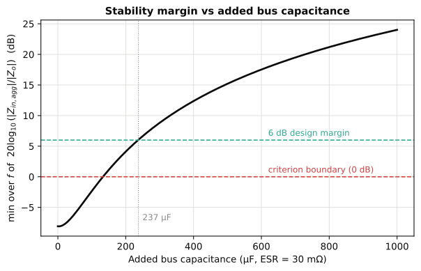
For this example, sweeping added bus capacitance against the worst-case margin (Fig. 11) shows the system crossing the criterion boundary at around 100µF and reaching a 6 dB margin at roughly 240µF of added bulk (30mΩ series resistance). The shape of the curve matters: steep at first, then flattening. Beyond a point, more capacitance buys little, because the residual peak is set by the damping resistance rather than by the resonant frequency.
Measuring and simulating the impedances
The criterion is only as good as the two curves you compare.
Simulation. Both impedances come from AC injection at the interface. For : inject a small AC current into the source's output with the load replaced by its bias-point equivalent, and plot . For : the same at the load's input. The detail that decides whether the result means anything is that the converter's must be simulated closed loop, with an average model (or a SIMPLIS/periodic small-signal analysis) and the full compensator in place. The negative-resistance behaviour is a product of regulation. Simulate the power stage open loop, or with the output unregulated, and you'll see a benign positive impedance and conclude, wrongly, that there is nothing to worry about. This is probably the single most common way the analysis goes quietly wrong.
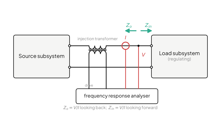
Bench. The interface impedances are measured with a frequency response analyser and an injection transformer (or a four-terminal impedance analyser at low power): break the connection, insert a small wideband injection resistor or transformer, sweep, and compute the impedance from the voltage and current at the interface (Fig. 12). Measure at the operating point. scales with , so worst case is minimum input voltage at maximum load, and that's where the measurement and the design margin both matter most.
One criterion, three shapes of trouble
| Scenario | What looks like | What looks like | Primary fix |
|---|---|---|---|
| Input filter | High-Q peak at the passive LC resonance | flat, rising above loop bandwidth | Damping snubber: – across by default; – across if capacitance is constrained |
| Cascaded stages | Peak near the source converter's crossover, worst with voltage mode and low phase margin | Single load's | Damped bulk capacitance at the interface, with a controlled damping resistance rather than hoped-for ESR |
| Distribution bus | As the cascade, plus interconnect inductance seen per-load | : admittances add | Check against the parallel load impedance; budget admittance per load; size bus capacitance for margin |
The discipline is the same in every case. Plot and on the same axes at the worst-case operating point and keep 6 dB of daylight between them. And remember that the load side gets lower every time someone adds a converter to the rail.
The plots in this article were generated from the component values quoted, using simplified closed-loop models (; with a first-order loop). They illustrate the mechanisms; for design sign-off, extract the impedances from your actual compensated models as described above. Doing that across a real system, with each converter's compensated small-signal model, the interface impedances overlaid automatically, and the damping components carried at their worst-case values over temperature rather than their room-temperature datasheet numbers, is exactly the analysis switchmode.io is being built to do. The impedance overlay is where the design conversation starts; the tolerance corners are where it gets signed off.
References
[1] R. D. Middlebrook, "Input Filter Considerations in Design and Application of Switching Regulators," IEEE Industry Applications Society Annual Meeting, 1976.
[2] Texas Instruments, "Demystifying Type II and Type III Compensators Using Op Amp and OTA for DC/DC Converters." [Online]. Available: https://www.ti.com/lit/an/slva662/slva662.pdf
[3] R. W. Erickson and D. Maksimović, Fundamentals of Power Electronics, 3rd ed., Springer, 2020. Ch. 17 (input filter design and damping networks).