I costed 30 MOSFETs in the same 48V to 12V, 6A buck converter, one pair at a time, with every loss in the power stage included. The most efficient was the smallest die in the library, Infineon's 12.1mΩ ISC151N08NM6, at 93.3%. Its 1.5mΩ sibling from the same family lost 7.0W more. The lowest-resistance part of all, at 0.84mΩ, lost 35W delivering 72W.
The Buck Converter Losses Nobody Tells You About ends by recommending a loss budget that includes every mechanism from the start. This is that budget for one 48V design, costed in milliwatts on parts you can buy. It shows why the usual selection rule, the lowest on-resistance you can afford, fails at this bus voltage in both switch positions.
The converter
| Parameter | Value |
|---|---|
| Input | 48V |
| Output | 12V, 6A (72W) |
| Switching frequency | 500kHz |
| Inductor | Murata DD1274AS-H-5R6N, 5.6µH (5.46µH at bias, 3.30A ripple) |
| Input capacitors | 4 × Murata GRM31CZ72A475KE11, 4.7µF 100V X7R 1206 |
| Output capacitors | 4 × Murata GRM32ER71E226KE15, 22µF 25V X7R 1210 |
| Gate drive | 7.5V, from a 2Ω pull-up and 1Ω pull-down driver |
| Dead time | 30ns on both edges |
| Ambient | 40°C |
| Thermal path | 50K/W junction to ambient, the datasheets' own figure for 6cm² of copper |
The bus and the frequency are the same as in the MOSFET Coss loss app note and the RC snubber app note. The 7.5V drive is what a 48V controller such as the TI LM5145 provides [4].
Every MOSFET sits in both positions, the same part as high side and low side, unless a table says otherwise. The part data comes from switchmode.io's component catalogue, read from each datasheet's own curves. The losses come from the analysis engine switchmode.io is being built on. It solves each switch's junction temperature against its own loss, so on-resistance is read hot. Three tables need conditions outside that run: other bus voltages, other inductors and a different gate supply. Those come from my own independent model of the same terms. It agrees with the engine to 0.3 points on the five best parts.
The budget on the obvious part
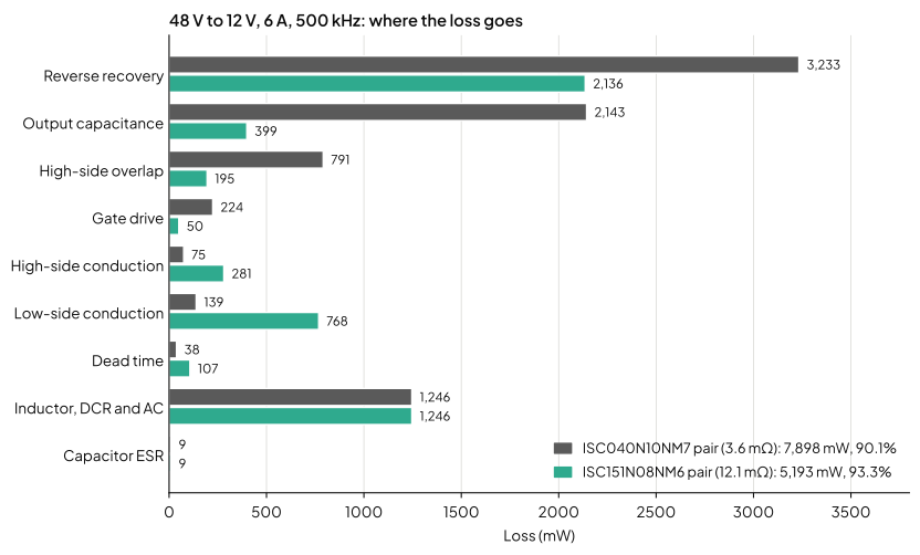
ISC040N10NM7 is the part I'd have reached for first. It's 100V, it's 3.6mΩ, and the Coss app note uses it on this same bus. Here is where its 7.9W goes, beside the part that wins.
| Loss term (mW) | ISC040N10NM7 pair | ISC151N08NM6 pair |
|---|---|---|
| Reverse recovery | 3,233 | 2,136 |
| Output capacitance | 2,143 | 399 |
| High-side switching overlap | 791 | 195 |
| Gate drive | 224 | 50 |
| High-side conduction | 75 | 281 |
| Low-side conduction | 139 | 768 |
| Dead time | 38 | 107 |
| Inductor DCR / AC | 649 / 597 | 649 / 597 |
| Input and output capacitor ESR | 9 | 9 |
| Total | 7,898 | 5,193 |
| Efficiency | 90.1% | 93.3% |
On ISC040N10NM7, conduction is 2.7% of the loss. Four terms that are paid in charge make up 81%. They're the output capacitance, the reverse recovery, the switching overlap and the gate drive. Each one is set by charge moved once per cycle, so each scales with the switching frequency. The first three also scale with the bus voltage. Conduction scales with neither.
The output-capacitance term is the high side charging the low side's output capacitance from the bus at every turn-on. It also dumps its own stored energy in its channel [1]:
where:
- is the output-capacitance loss, in watts, all of it in the high side
- and are the energies stored in the high side's and low side's output capacitance at , in joules
- is the low side's output charge at , in coulombs
- is the input voltage, 48V
- is the switching frequency, 500kHz
With the same part in both positions the two energies cancel. ISC040N10NM7 holds 89.1nC at 48V, so the term is 89.1nC × 48V × 500kHz = 2.14W. The Coss app note derives it in full.
Reverse recovery works the same way. The high side's turn-on sweeps the stored charge out of the low side's body diode, against the full bus:
where is the reverse-recovery loss in watts, and is the low side's recovered charge at the edge's current slew rate, in coulombs. and are as above. The engine reads as 135nC on ISC040N10NM7, which gives 3.23W. That figure is the least certain in the budget, and the section on it below explains why.
Then the swap. ISC151N08NM6 has 3.4 times the on-resistance , the channel's resistance when it's fully on. Conduction rises by 835mW. The four charge terms fall by 3,607mW. The high side's share is the part that matters most. It drops from 5.8W to 2.2W.
What is the most efficient MOSFET for a 48V buck?
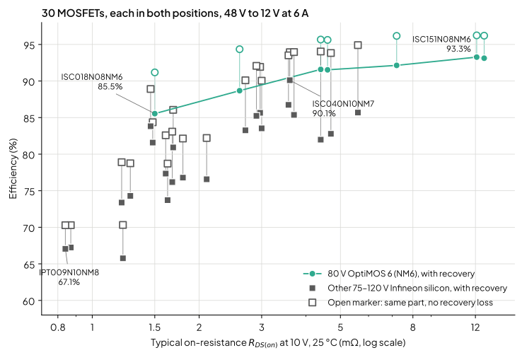
The smallest die that carries the current. At 6A from 48V that's the 12.1mΩ ISC151N08NM6, in both positions. Its 12.7mΩ sibling in a smaller package, ISZ157N08NM6, is a close second. Fig. 2 and the table show all 30 parts, each in both positions. The table gives each part's and its output charge at 48V. It also gives the recovery charge the engine reads for it.
| Part | Rating | (mΩ) | at 48V (nC) | (nC) | Efficiency | Without |
|---|---|---|---|---|---|---|
| ISC151N08NM6 | 80V | 12.1 | 16.6 | 89 | 93.3% | 96.2% |
| ISZ157N08NM6 | 80V | 12.7 | 16.7 | 89 | 93.1% | 96.2% |
| ISC088N08NM6 | 80V | 7.2 | 28.1 | 129 | 92.1% | 96.2% |
| ISZ053N08NM6 | 80V | 4.4 | 44.5 | 135 | 91.6% | 95.7% |
| ISC056N08NM6 | 80V | 4.6 | 44.5 | 136 | 91.5% | 95.6% |
| ISC040N10NM7 | 100V | 3.6 | 89.1 | 135 | 90.1% | 93.9% |
| ISC031N08NM6 | 80V | 2.6 | 78.4 | 202 | 88.7% | 94.4% |
| ISC040N10NM8 † | 100V | 3.57 | 89.4 | 247 | 86.7% | 93.5% |
| IPP062NE7N3 | 75V | 5.6 | 49.1 | 340 | 85.7% | 94.9% |
| ISC033N10NM8 † | 100V | 2.97 | 108.4 | 237 | 85.7% | 91.9% |
| ISC018N08NM6 | 80V | 1.5 | 136.0 | 216 | 85.5% | 91.2% |
| BSC042NE7NS3 | 75V | 3.7 | 60.1 | 319 | 85.4% | 94.0% |
| BSC036NE7NS3 | 75V | 2.9 | 74.7 | 260 | 85.2% | 92.1% |
| ISC016N08NM8 | 80V | 1.46 | 163.1 | 204 | 83.8% | 88.9% |
| IPP034NE7N3 | 75V | 3.0 | 103.9 | 259 | 83.5% | 90.0% |
| IPB031NE7N3 | 75V | 2.7 | 103.9 | 273 | 83.3% | 90.1% |
| IPP052NE7N3 | 75V | 4.7 | 60.7 | 423 | 82.8% | 93.8% |
| IPB049NE7N3 | 75V | 4.4 | 60.7 | 466 | 82.0% | 94.0% |
| IPTC017N12NM6 | 120V | 1.48 | 233.3 | 121 | 81.6% | 84.4% |
| ISC019N10NM8 † | 100V | 1.69 | 195.2 | 221 | 80.9% | 86.1% |
| IPT018N10NM8 † | 100V | 1.61 | 226.5 | 246 | 77.3% | 82.6% |
| IPB020NE7N3 | 75V | 1.8 | 182.9 | 254 | 76.8% | 82.1% |
| IPP023NE7N3 | 75V | 2.1 | 182.9 | 269 | 76.6% | 82.2% |
| IPF019N10NM8 † | 100V | 1.68 | 226.1 | 327 | 76.2% | 83.1% |
| IPF014N10NM8 † | 100V | 1.28 | 296.8 | 229 | 74.3% | 78.8% |
| IPB018N10NM8 † | 100V | 1.63 | 296.8 | 259 | 73.7% | 78.7% |
| IPT014N10NM8 † | 100V | 1.21 | 295.9 | 286 | 73.4% | 78.9% |
| IPF009N10NM8 † | 100V | 0.87 | 480.7 | 194 | 67.2% | 70.3% |
| IPT009N10NM8 † | 100V | 0.84 | 475.2 | 206 | 67.1% | 70.3% |
| IPB013N10NM8 † | 100V | 1.22 | 480.7 | 296 | 65.8% | 70.3% |
is the datasheet's typical on-resistance at 10V and 25°C. is the output charge at 48V, integrated from the datasheet's output-capacitance curve unless marked. is the charge the engine reads for that part at its own edge rate.
† The 100V OptiMOS 8 datasheets publish a curve, and the table uses it. It reads about 2.6 times what integrating the same datasheet's capacitance curve gives. Treat those parts' positions as approximate. Even the integral leaves IPT009N10NM8 at 186nC, eleven times ISC151N08NM6.
The cleanest comparison is inside one family. The 80V OptiMOS 6 parts share a generation, a voltage and a datasheet format. From 1.5mΩ to 12.1mΩ their efficiency climbs from 85.5% to 93.3%. The only exception is a 0.06-point tie between the 4.4mΩ and 4.6mΩ parts. With no reverse recovery at all, it climbs from 91.2% to 96.2%. The order doesn't change.
Across families, the order tracks charge. The 75V NE7N3 parts publish one recovery figure each, 58 to 129nC at 100A/µs. The NM6 parts publish 16 to 54nC, and the NE7N3 parts sink. The 100V parts carry more output charge for the same resistance. times is about 200nC·mΩ on the 80V NM6 parts and about 320nC·mΩ on the 100V ones. So sort by charge first, and use resistance as the tiebreaker.
What if the design needs 100V parts? The smallest 100V die in the catalogue I used is 3.6mΩ. That's ISC040N10NM7, at 90.1%, and its OptiMOS 8 successor. ISC151N08NM6 is an 80V part, run at 60% of its rating. That's normal for a regulated 48V rail. It isn't enough for a telecom bus that runs to 60V before it rings. GaN is the other answer. In my independent model, the best CoolGaN pair reaches about 96.5%, because a GaN switch has no body diode to recover. Its high side is the smallest GaN die in the set.
The low side too
Why the Lowest RDS(on) Isn't the Best MOSFET for Your Buck Converter splits the job in two. The high side wants low charge. The low side wants the lowest on-resistance you can fit, because it conducts for most of the cycle. That's right for its 12V to 1.8V, 20A converter. At 48V the low-side half fails too.
Hold ISC151N08NM6 on the high side and sweep the low side:
| Low side | (mΩ) | Low-side conduction (mW) | Recovery loss (mW) | High-side total (mW) | Efficiency |
|---|---|---|---|---|---|
| ISC151N08NM6 | 12.1 | 768 | 2,136 | 2,152 | 93.3% |
| ISC088N08NM6 | 7.2 | 430 | 3,096 | 2,996 | 92.2% |
| ISZ053N08NM6 | 4.4 | 281 | 3,240 | 3,494 | 91.9% |
| ISC040N10NM7 | 3.6 | 142 | 3,250 | 4,657 | 91.4% |
| ISC018N08NM6 | 1.5 | 98 | 6,864 | 7,685 | 86.5% |
| IPT009N10NM8 | 0.84 | 53 | 19,320 | 25,721 | 69.5% |
Each step to a lower-resistance low side saves the low side tens or hundreds of milliwatts, and costs the high side more. Going from 12.1mΩ to 7.2mΩ saves 338mW of conduction and adds 844mW to the high side. The loss moves to the switch that was already hottest. The selection article calls this the loss showing up in the wrong device. At 48V it decides the selection.
With no reverse recovery at all, the 7.2mΩ low side edges the 12.1mΩ one by 0.1 points. So state the rule as the smallest die, or the next one up. The 1.5mΩ low side still costs two points there.
Where does the old rule come back? My independent model picked the best pair from the five NM6 parts at 25% duty. It counts switch loss only, so the high-current cases don't need a real inductor. Each entry is a part's typical :
| Input | 6A | 12A | 20A |
|---|---|---|---|
| 12V | High 4.4mΩ, low 4.4mΩ | High 4.4, low 4.4 | High 4.4, low 1.5 |
| 24V | High 12.1, low 12.1 | High 4.4, low 4.4 | High 4.4, low 2.6 |
| 48V | High 12.1, low 12.1 | High 12.1, low 4.4 | High 4.4, low 4.4 |
At 12V and 20A, the lowest-resistance low side wins, which is the selection article's own territory. Raise the bus or lower the current and the best low side shrinks. At 48V the lowest-resistance part never wins, even at 20A. Duty cycle pushes the same way: the selection article ran at 15%, where the low side conducts for longer than it does here.
Why the charge terms win at 48V
On the ISC040N10NM7 pair, the output-capacitance loss is 181mW from a 12V bus and 2,139mW from 48V. That's 11.8 times for four times the voltage. It isn't the sixteen times that a fixed capacitance would give, because the output capacitance falls as the voltage rises. Reverse recovery scales linearly with the bus, and the overlap at least as fast. Gate drive follows the drive voltage. Conduction doesn't change at all.
That explains the contrast with the published 12V budgets. Microchip's AN1471 costs a 12V to 1.2V, 20A converter on real parts, and output capacitance comes out at 1.1% of its loss [7]. Here it's 27%. Same mechanism, opposite conclusion.
The same terms scale with frequency. From 500kHz to 1MHz, the ISC151N08NM6 pair loses 3.3 points and the ISC040N10NM7 pair loses 6.7. A small die is what makes a higher switching frequency affordable at 48V.
The efficiency curve
| Load | ISC040N10NM7 pair | ISC151N08NM6 pair |
|---|---|---|
| 100% (6A) | 90.1% | 93.3% |
| 75% | 89.4% | 92.7% |
| 50% | 87.5% | 90.8% |
| 25% | 82.6% | 94.1% |
| 10% | 65.0% | 90.3% |
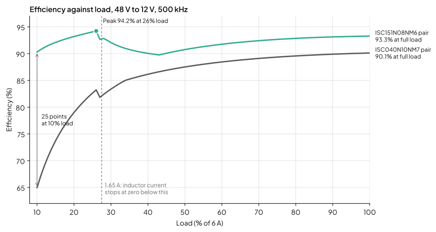
The gap grows from 3 points at full load to 25 points at 10%. The big pair's 2.1W of output-capacitance loss and its gate drive don't fall with load. At 0.6A they're most of what it loses. Infineon makes the same point about synchronous rectifiers. Switching and gate losses "do not vary with load", while conduction falls with the square of the current [2].
The curve assumes the controller lets the inductor current stop at zero below 1.65A, so the converter runs discontinuous there. A controller that forces continuous conduction keeps the current circulating at light load [8]. One that skips pulses at light load saves part of the switching loss on top [5]. Check which your controller does before you compare against these numbers.
What the budget doesn't tell you
The high side's temperature. Take the datasheets' own 50K/W. ISC040N10NM7's high side dissipates 5.8W and solves to 332°C, nearly twice its 175°C limit. ISC151N08NM6's high side dissipates 2.2W and solves to 148°C. That's inside its limit, with less margin than most designers would sign off. Your board won't match the datasheet's. The 2.7 times difference in high-side dissipation holds on any board.
The gate supply. The gate drive above assumes the 7.5V comes from somewhere free. A 48V controller usually makes it with a linear regulator from the input. The LM5145's regulator runs from up to 75V and sets its output to 7.5V [4]. Every coulomb of gate charge then comes from 48V, and the regulator dissipates the difference. My independent model puts the ISC040N10NM7 pair's gate loss at 224mW from a free rail. Through the regulator it's 1,433mW, and 1.4 points of efficiency. The small pair loses 0.3 points. The datasheet's fix is a diode from the output. The regulator's dissipation "can be minimized by connecting the output voltage or an auxiliary bias supply rail (up to 13 V) to VCC" [4]. A 12V output is inside that limit.
The reverse-recovery charge. It's the biggest term in both budgets, and the one I trust least. I found out how badly a comparison can go the first time I ran this design. ISC151N08NM6's datasheet gives at two current slew rates: 16nC at 100A/µs and 89nC at 1,000A/µs [6]. ISC040N10NM7's gives one: 23nC at 100A/µs [3]. Read side by side, the 3.6mΩ part looks like it recovers a quarter of the charge. Read at the same slew rate, on the engine's estimate, it recovers about 1.5 times as much. When I first ran this design, the engine took each datasheet's nearest line, so the low-side comparison came out the wrong way round. Now the engine reads every part at the same rate. It carries a single line to that rate by the slope measured on parts that publish two.
The remaining uncertainty runs both ways. The edges here commutate at about 1,000A/µs on the big part and 4,400A/µs on the small one. Recovery charge keeps rising with slew rate, so the small part's figure may read low. But the datasheet test conducts the diode for far longer than the 30ns dead time here. Infineon also says its JEDEC figure "includes not only the body diode Qrr but also a part of the output charge" [2]. Nexperia states for its own parts [9]. Here is the recovered charge, the stored charge and the output charge. So part of this term repeats the output-capacitance term. That's why the ranking table carries a second column with no recovery at all. ISC151N08NM6 is first in both, and it beats ISC040N10NM7 by 3.2 points with recovery and 2.3 without.
The edges. The gate-charge model has no loop inductance. On ISC151N08NM6 it gives a 3.7ns turn-on and a 1.8ns turn-off. Real edges will be slower and ring. If the overlap loss tripled, the small pair would still lead by more than two points. The ringing is what the snubber app note is for. The turn-off figure also counts the switching node's capacitance. As the channel turns off, the inductor current charges the node, so the voltage across the switch lags the current [10]. On the big part, the simple estimate of half the voltage times the current times the turn-off time would add about 0.7W.
The inductor. Ten of the 31 Murata inductors I checked fit this design inside their current ratings. On the best pair, my independent model puts all ten within 84mW of each other. The MOSFET choice spans 32W. Spend the selection time where the spread is.
Running your own pair
None of this needs exotic parts. It needs each charge term costed at the bus voltage you actually run, on both switches at once, with the temperature solved. The MOSFET power loss calculator runs the switch terms for any pair.
This page is one operating point, one inductor and one board figure, and that's what it leaves undone. A real selection has to hold across the input and load ranges, at the board's real temperature, with the controller that drives it. It has to be redone when any of those change. switchmode.io is being built to rerun the whole ranking whenever one of those assumptions moves.
References
[1] A. Gorgerino, "Hard Switching Losses Calculations," Efficient Power Conversion Corp., Appl. Note AN030, 2024. [Online]. Available: https://epc-co.com/epc/Portals/0/epc/documents/application-notes/AN030%20Hard%20Switching%20Losses%20Calculation.pdf
[2] P. B. Green, S. Mazzer, O. Guillemant, C. Moesslacher and K. Ream, "OptiMOS device selection for synchronous rectification," Infineon Technologies AG, Appl. Note AN_2212_PL15_2301_094414, V1.1, Feb. 2023. [Online]. Available: https://www.infineon.com/dgdl/Infineon-MOSFET_OptiMOS_device_selection_for_synchronous_rectification-ApplicationNotes-v01_00-EN.pdf?fileId=8ac78c8c85ecb34701865afe0f7d3f05
[3] Infineon Technologies AG, "ISC040N10NM7 OptiMOS 7 Power-Transistor, 100 V," datasheet, Rev. 1.0, Nov. 2025. [Online]. Available: https://www.infineon.com/assets/row/public/documents/24/49/infineon-isc040n10nm7-datasheet-en.pdf
[4] Texas Instruments, "LM5145 6-V to 75-V Synchronous Buck DC/DC Controller With Wide Duty Cycle Range," SNVSAI4B, Nov. 2017, rev. Nov. 2020, §8.3.3. [Online]. Available: https://www.ti.com/lit/ds/symlink/lm5145.pdf
[5] S. Jaffe and K. Wiggenhorn, "Understanding Mode Transitions for LMR33620/30 and LMR36006/15," Texas Instruments, Appl. Rep. SNVA857, Apr. 2019. [Online]. Available: https://www.ti.com/lit/pdf/snva857
[6] Infineon Technologies AG, "ISC151N08NM6 OptiMOS 6 Power-Transistor, 80 V," datasheet, Rev. 2.0, Mar. 2023. [Online]. Available: https://www.infineon.com/assets/row/public/documents/24/49/infineon-isc151n08nm6-datasheet-en.pdf
[7] J. Depew, "Efficiency Analysis of a Synchronous Buck Converter using Microsoft Office Excel-Based Loss Calculator," Microchip Technology Inc., Appl. Note AN1471, 2012. [Online]. Available: https://ww1.microchip.com/downloads/en/Appnotes/01471A.pdf
[8] D. Jauregui, B. Wang and R. Chen, "Power Loss Calculation With Common Source Inductance Consideration for Synchronous Buck Converters," Texas Instruments, Appl. Rep. SLPA009A, Jul. 2011. [Online]. Available: https://www.ti.com/lit/pdf/slpa009a
[9] Nexperia B.V., "Understanding power MOSFET data sheet parameters," Appl. Note AN11158, Rev. 7.0, Feb. 2025. [Online]. Available: https://assets.nexperia.com/documents/application-note/AN11158.pdf
[10] D. Perreault, "Lecture 15 – Switching losses and snubbers," MIT 6.622 Power Electronics, Spring 2023, MIT OpenCourseWare. [Online]. Available: https://ocw.mit.edu/courses/6-622-power-electronics-spring-2023/mit6_622_s23_lec152.pdf