A synchronous buck has two dead times, and they aren't the same problem. This note sets each one from the MOSFET datasheets and the gate driver's datasheet. Then it checks the answers against a simulation that uses the MOSFET vendor's own models. It covers hard-switched silicon MOSFETs in continuous conduction. The worked example is the 48 V to 12 V, 500 kHz converter from MOSFET Coss Loss in a Half-Bridge: Which Switch Pays, and How Much.
The result
Call the interval from the high side's gate command going low to the low side's going high the high-side edge. The other interval, low side off to high side on, is the low-side edge.
- The high-side edge has an optimum, and it moves with load. The inductor current has to move the switch node from the input rail to ground before the low side turns on. That takes longer at light load. Too short and the low side turns on into a node that's still charged. Too long and the body diode conducts. Being short costs 10 to 22 times more per nanosecond than being long, so set this edge long, for the lightest load you care about.
- The low-side edge has no optimum, only a floor. The node is already at the bottom rail, so the body diode conducts for all of this dead time past one fixed point. Set it as short as the gate timing and the driver allow. In the 48 V simulation, each extra nanosecond cost as much as a 7 V drop at the inductor current would. The diode's own drop is 0.88 V. The rest is charge the diode stores and the high side then has to remove.
In the worked example this gives 43 ns on the high-side edge and 12.5 ns on the low-side edge. Against a single 17.8 ns on both, from Infineon's delay-difference rule, that saves 0.39 W at full load and 0.36 W at light load. Against a 50 ns default it saves 2.05 W at full load. The converter delivers 200 W.
Why the two edges differ
Fig. 1 shows both edges of the worked example at full load, each with the same 30 ns between gate commands.
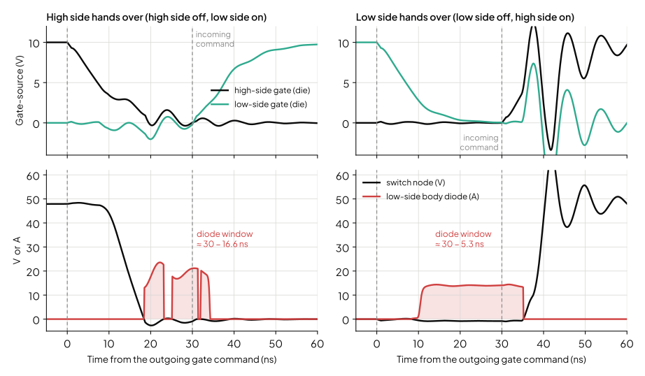
The high-side edge. The high side's gate falls for about 10 ns before its channel lets go of the current. Then the inductor current discharges the node from 48 V to ground, through both switches' output capacitances. The body diode conducts only after that. So part of the dead time goes on the gate and part on the node, and only the rest is diode conduction. The node's part depends on the load current.
The low-side edge. The low side's gate also takes about 10 ns to fall. But the node doesn't move when the channel lets go. The inductor current still flows out of the node, so the body diode picks it up at once, with the node at about −0.8 V. It conducts until the high side's channel has taken over the whole current. Nothing about the load changes that.
A dead-time rule that treats the two edges alike, such as the slowest turn-off delay plus a margin, is right for at most one of them.
What you need
From each MOSFET datasheet:
- The internal gate resistance .
- The minimum gate threshold voltage and the plateau voltage .
- The gate-drain charge .
- The gate charge with no drain voltage, , often called "gate charge total, sync. FET". If your datasheet doesn't give it, read the total gate charge at your drive voltage off the gate-charge curve.
- The output capacitance curve, or the output charge curve.
- The body diode's forward voltage .
From the gate driver's datasheet: the drive voltage , the pull-up and pull-down resistances, and the delay matching between the high and low outputs, . Use its maximum. If the driver gives no resistances, work them out from its output voltage drops at a stated current.
From the converter: the input voltage , and the inductor current at each edge at every load you care about. The high side turns off at the peak current . The low side turns off at the valley current .
Don't use the datasheet's turn-on and turn-off delays, and . Each is measured at one gate resistance and one gate voltage, and usually into a resistive load [1]. The end points are on the drain voltage, not on the channel current [2]. Your driver isn't the test fixture. For the worked example's MOSFET, Infineon's own model gives a turn-off delay of 10.5 ns at the datasheet's test conditions. The datasheet says 17.2 ns.
Step 1 Work out the gate timing
The outgoing switch's channel lets go when its gate has fallen to the threshold. The incoming switch's channel starts to conduct when its gate has risen to the threshold. Treat each gate as a resistor charging a capacitor:
where:
- is the time from the outgoing gate command to its channel letting go of the current.
- is the time from the incoming gate command to its channel starting to conduct.
- is the driver's pull-down resistance plus any external gate resistor plus .
- is the driver's pull-up resistance plus any external gate resistor plus .
- is the input capacitance with no drain voltage. is the gate voltage the datasheet measured at, usually 10 V.
- is the driver's output voltage.
- is the minimum gate threshold voltage.
The low-side edge needs one more number. The high side doesn't carry the whole current until its gate reaches the plateau:
where is the time from the high side's gate command to its channel carrying the whole current, is its plateau voltage, and , and are as above.
Use the minimum threshold in both. A low threshold makes a turn-off longer and a turn-on shorter, and both of those make the dead time you need longer. So the minimum gives you the safe answer on both edges. The datasheet's minimum is at 25 °C, and the threshold falls as the junction heats. If your switches run hot, take the threshold from the datasheet's threshold-against-temperature plot.
Step 2 Work out the node transit on the high-side edge
After the high side's channel lets go, something has to move the node from the input rail to ground. Either the inductor current moves it, or the high side's gate holds it back:
where:
- is the time the node takes to fall from to ground.
- is the charge in both switches' output capacitances at the input voltage. Integrate it from the curves as in Step 2 of MOSFET Coss Loss in a Half-Bridge: Which Switch Pays, and How Much. Add any other capacitance on the node, such as a snubber's.
- is the inductor current when the high side turns off.
- is the high side's gate-drain charge, is its gate's turn-off resistance from Step 1, and is its plateau voltage.
The first term is the charge-limited transit. The channel is already off, and the inductor current alone discharges the node. The second is the gate-limited transit. The gate can't fall through its plateau any faster than its driver can pull the gate-drain charge out, so the node can't move faster either. In that case the channel carries current all the way across, which is turn-off loss on top.
Christen and Biela derive the boundary between the two, including the effect of source inductance [3]. Ignoring source inductance, and in the datasheet's charge terms, the transit is gate-limited above
where is the current at which the two transits are equal, and , , and are as above.
TI's SLPA009A, a common reference for buck losses, treats the high side's turn-off as always gate-limited [4]. That's right only above .
Step 3 Set the high-side edge
The dead time at which the low side turns on just as the node arrives at ground is:
where:
- is the zero-window dead time on the high-side edge, gate command to gate command.
- is the high side's turn-off time from Step 1.
- is the node transit from Step 2.
- is the low side's turn-on time from Step 1.
Shorter than , and the low side turns on into a node that still holds charge. Its channel dumps that charge, and at worst that's the whole hard-switching energy of the turn-on. For two switches that are the same part, that's per cycle, where is one switch's output charge at the input voltage . Longer than , and the body diode conducts for the difference. That costs per nanosecond, per cycle.
The first cost is much the larger. So set
where:
- is the dead time you set on the high-side edge.
- is the zero-window dead time at the lightest load at which you want this edge to be soft. That's where the transit is longest.
- is the driver's maximum delay matching between its two outputs.
The matching appears because the driver can delay its two outputs by different amounts. That shortens one edge and lengthens the other, and the datasheet doesn't say which [5]. Below that lightest load the transit grows past any sensible dead time, and the edge goes partly hard.
Step 4 Set the low-side edge
There's no transit to wait for. The diode starts to conduct as soon as the low side lets go, and it stops when the high side carries the whole current:
where:
- is the zero-window dead time on the low-side edge, gate command to gate command.
- is the low side's turn-off time from Step 1.
- is the time from the high side's gate command to its channel carrying the whole current, from Step 1.
Then set
where is the dead time you set on the low-side edge and is the driver's maximum delay matching.
doesn't depend on the load. Below it, the high side starts to conduct before the low side has let go. The first part of that overlap only takes back the low side's reverse current, so a nanosecond or two of it isn't shoot-through. But you can't aim there with a driver whose matching is several nanoseconds.
Above , each nanosecond costs at least per cycle. At 48 V it costs much more. The diode stores charge the whole time it conducts, and the high side removes that charge against the full input voltage when it turns on. The datasheet's reverse recovery charge can't tell you how much. It's measured after a long conduction and at a slow current ramp, 100 A/µs for the worked example's switch. So keep this edge short. The worked example shows the size of the effect.
Step 5 Check a controller's fixed dead times
A controller with integrated drivers sets the dead times for you. Run Steps 1 to 4 with its driver's resistances, then compare:
where:
- and are the body diode's conduction times on the two edges.
- and are the controller's dead times on the two edges.
- and are the zero-window dead times from Steps 3 and 4.
A negative means the high-side edge goes partly hard at that load. A negative means the two switches overlap. Positive windows cost at least
where is the body diode's conduction loss, is its forward voltage, and are the inductor currents at the two edges, and are the windows from above, and is the switching frequency. On the low-side edge, stored charge comes on top.
Read the controller's definition before you compare. Some give a fixed delay between their gate pins at 50% of the swing, into a stated capacitance. If that capacitance is close to your switch's , the number is a few nanoseconds from the command-to-command interval this note uses.
An adaptive controller waits for the outgoing gate pin to fall below a threshold, then adds a fixed delay. On the LM5143-Q1 that's 2.5 V plus 22 ns [6]. There, check that the switch's own gate is below when the pin crosses the controller's threshold. The internal gate resistance makes the switch's gate lag its pin, and TI warns that an external gate resistor shortens the effective dead time [6].
Worked example: 48 V to 12 V at 500 kHz
The converter. An Infineon ISC040N10NM7 in both positions [7], 48 V to 12 V at 500 kHz. A 3.3 µH inductor gives 5.45 A of ripple. Three loads: 16.7 A (full, 200 W), 8.35 A (half) and 4.0 A (light). The high side turns off at 19.4 A, 11.1 A and 6.7 A. The low side turns off at 14.0 A, 5.6 A and 1.3 A.
The driver. A TI UCC27282 at 10 V, with no external gate resistors [5]. Its datasheet gives output drops at 100 mA. They work out to 1.3 Ω pull-up, and 1.0 Ω (high output) and 0.85 Ω (low output) pull-down. Its delay matching is 7 ns maximum.
From the MOSFET datasheet: = 1.3 Ω, = 2.3 V, = 4.7 V, = 6.8 nC, = 35 nC at 10 V, so = 3.5 nF. = 0.88 V.
- Gate timing. = 1.0 + 1.3 = 2.3 Ω, so = 2.3 Ω × 3.5 nF × ln(10/2.3) = 11.8 ns. = 1.3 + 1.3 = 2.6 Ω, so = 2.4 ns. = 0.85 + 1.3 = 2.15 Ω, so = 11.1 ns. The high side reaches its plateau in = 5.8 ns.
- Transit. Each switch holds 89.1 nC at 48 V, so = 178.3 nC. The gate-limited transit is 6.8 nC × 2.3 Ω / 4.7 V = 3.3 ns, and = 53.6 A. So the transit is charge-limited at every load: 9.2 ns at full load, 16.1 ns at half and 26.5 ns at light.
- High-side edge. = 11.8 + 9.2 − 2.4 = 18.6 ns at full load, 25.5 ns at half and 36.0 ns at light. Set for light load: = 36.0 + 7 = 43 ns. Erring short here could cost up to the full hard turn-on, 4.28 µJ, which is 2.14 W at 500 kHz. Erring long costs 0.88 V × 19.4 A = 17 nJ per nanosecond at full load.
- Low-side edge. = 11.1 − 5.8 = 5.3 ns at every load. = 5.3 + 7 = 12.3 ns, so set 12.5 ns.
Against the alternatives. Infineon's dead-time rule for IGBTs is 1.2 times the turn-off delay minus the turn-on delay, plus the driver's delay spread [8]. With this datasheet's typical delays and the 7 ns matching, it gives 1.2 × [(17.2 − 9.4) + 7] = 17.8 ns on both edges. The loss differences below come from the simulation described later, at 500 kHz.
| Dead times (high-side / low-side edge) | Full load, 200 W | Half load, 100 W | Light load, 48 W |
|---|---|---|---|
| This note: 43 / 12.5 ns | reference | reference | reference |
| One rule for both: 17.8 / 17.8 ns | +0.39 W | +0.15 W | +0.36 W |
| 50 / 50 ns | +2.05 W | +0.85 W | +0.20 W |
The single 17.8 ns is better than 43 ns on the high-side edge at full load, by 0.18 W. It loses 0.57 W on the low-side edge at the same load. At light load it turns the low side on 13 ns early, and that costs 0.30 W, which is 0.6% of the output power.
What the margins cost. Against the best high-side dead time the sweeps found, this note's 43 ns costs 0.22 W at full load. On the low-side edge, against its zero-window point, 12.5 ns costs 1.13 W. Nearly all of that is the 7 ns allowed for the driver's matching, which makes the matching the most expensive number in this design. The UCC27282's typical matching is 1 ns. A driver with a tighter maximum, or a controller that can trim each edge, is worth up to 1.1 W here at full load.
Worked example, run backwards: the same stage on an LTC7801
The LTC7801 is a 150 V buck controller with fixed dead times: 55 ns from top gate off to bottom gate on, and 50 ns from bottom gate off to top gate on [9]. They're measured at 50% levels into 3.3 nF, which is close to this MOSFET's 3.5 nF. Its drivers run at 10 V, with 2.2 Ω and 2.0 Ω pull-up and 1.0 Ω pull-down.
Steps 1 to 4 with its drivers give = 18.0 ns at full load and 35.3 ns at light, and = 4.1 ns. So:
- High-side edge: = 55 − 18.0 = 37 ns at full load and 20 ns at light. The edge stays soft at every load, and its diode costs 0.31 W at full load.
- Low-side edge: = 50 − 4.1 = 46 ns at every load. The diode drop alone accounts for 0.28 W at full load. The simulation puts it at 3.11 W.
That's 3.43 W in all at full load. It's more than the 2.14 W of capacitive loss that the Coss loss note found in the same converter. Fixed delays that long leave room for slow switches. With a fast 100 V switch at 48 V, they cost watts on the low-side edge.
A contrast: 12 V to 3.3 V, where the transit is gate-limited
Take an Infineon BSC009N04LSSC in both positions [10], 12 V to 3.3 V at 20 A and 500 kHz, with a 1.0 µH inductor. An LTC7803 drives it at 5.15 V, through 3.0 Ω pull-up and 1.5 Ω pull-down, with fixed 15 ns dead times [11]. The datasheet gives = 0.8 Ω, = 1.2 V to 2.0 V, = 2.4 V, = 15 nC and = 84 nC, so = 8.4 nF.
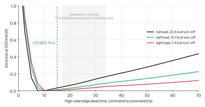
- The transit is gate-limited. = 124.5 nC at 12 V, so = 124.5 nC × 2.4 V / (15 nC × 2.3 Ω) = 8.7 A. At 22.4 A and 12.4 A the gate sets the transit, at 14.4 ns whatever the load. In the simulation the node takes 14 ns to 16 ns to fall from 90% to 10% at all three loads. A charge-only model gives 5.6 ns at full load.
- The threshold tolerance matters more than the load. With only 5.15 V of drive, runs from 17.0 ns at to 34.1 ns at . The simulation finds 21.3 ns. More drive voltage narrows that spread.
- Both edges are cheap. At 12 V a full hard turn-on costs only 0.75 µJ, which is 0.37 W at 500 kHz. In the simulation, any high-side edge from 7.5 ns to 25 ns costs no more than 0.10 W over the best at full load. The LTC7803's fixed 15 ns costs no more than 33 mW over the best, on either edge at any load.
So at low voltage, dead time is a floor to clear, not a number to tune. At 48 V the same procedure is worth watts.
Checking the procedure in simulation
I simulated each edge on its own in ngspice 45.2, with Infineon's level 1 models for both switches [12]. These include the package inductances and the internal gate resistance. The circuit adds 0.5 nH of power-loop inductance and 1 nH of gate-loop inductance. The inductor is an ideal current source at the edge current, because the inductor current barely moves in a few tens of nanoseconds. Every run starts and ends in the same state. So the energy from the input and the drivers, less the energy to the load, is the dissipation. I swept each dead time from 0 to 60 ns or 70 ns in 2.5 ns steps. That's three loads and three drive cases, 486 runs in all.
The netlists, sweep script and results are published with this note.
The zero-window points. The table compares the closed forms with the simulation. The simulated point is where the body diode's conduction time, extended back as a straight line, reaches zero.
| Edge | Converter | Closed form | Simulated, full / half / light load |
|---|---|---|---|
| High-side | 48 V, UCC27282 | 18.6 / 25.5 / 36.0 ns | 16.6 / 20.7 / 31.0 ns |
| High-side | 48 V, LTC7801 | 18.0 / 24.9 / 35.3 ns | 16.0 / 20.5 / 30.4 ns |
| High-side | 12 V, LTC7803 | 17.0 to 34.1 ns (threshold range), full and half load | 21.3 / 20.6 / 22.0 ns |
| Low-side | 48 V, UCC27282 | 5.3 ns | 5.3 / 5.5 / 5.5 ns |
| Low-side | 48 V, LTC7801 | 4.1 ns | 5.1 / 5.3 / 5.4 ns |
| Low-side | 12 V, LTC7803 | 8.1 ns | 6.7 / 7.7 / 9.4 ns |
On the high-side edge the closed form is long by 2 ns to 5 ns at 48 V. That's the safe side, and the minimum threshold is part of the reason. On the low-side edge it's no more than 1.4 ns out, either way.
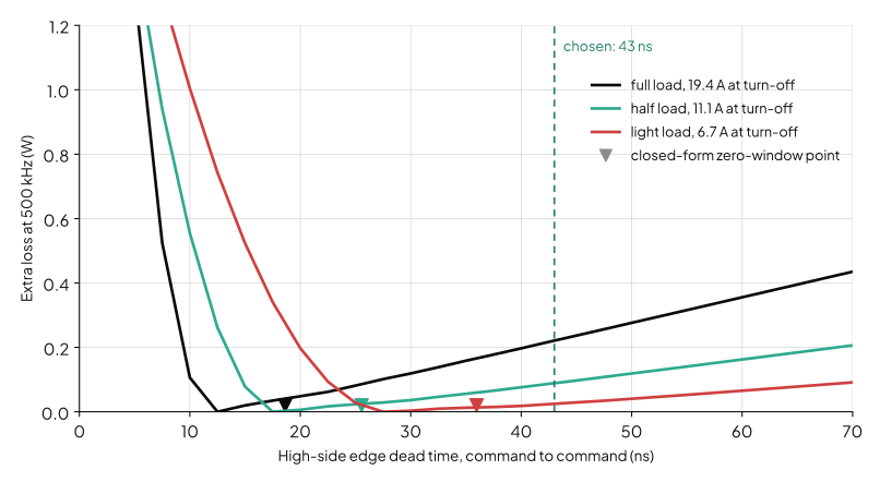
The cost of being wrong. On the high-side edge at 48 V, each nanosecond past the zero-window point costs 0.74 V to 0.81 V × , close to the 0.88 V diode drop. Each nanosecond short of the loss minimum costs 10 to 22 times as much. That asymmetry is why Step 3 errs long.
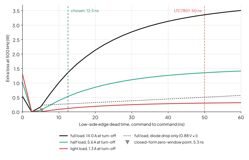
Stored charge on the low-side edge. At full load, take the extra loss over the zero-window point, less the diode drop, and divide it by 48 V. At 10 ns of dead time that's 31 nC. At 30 ns it's 99 nC, and at 60 ns it's 122 nC. The datasheet's is 23 nC, at 50 A and 100 A/µs.
This growth comes from the diode model in Infineon's OptiMOS 7 library, which builds charge over about 10 ns. I haven't measured it on hardware. The 40 V library models its diode with a fixed transit time, so it can't show the effect at all. The 12 V result's 0.6 V to 0.7 V × per nanosecond doesn't show that low-voltage parts escape it.
What the simulation doesn't check. It's consistent with itself, not with the datasheet. The models switch faster than their datasheets' tables say. At its datasheet's test conditions, the ISC040N10NM7 model gives a turn-off delay of 10.5 ns, against the table's 17.2 ns. The BSC009N04LSSC model gives 33.4 ns against 46 ns. A bench build of the 48 V converter is the next check, and this note will be revised with its results.
Assumptions and limits
- Continuous conduction, current flowing out of the node at both edges. If the valley current goes negative, as it can at light load in forced continuous mode, the low-side edge becomes soft and the roles swap. This procedure then doesn't apply to that edge.
- Silicon MOSFETs with a body diode. A GaN transistor has no reverse recovery, but it conducts in reverse at around 2 V with its gate off. So both windows cost more per nanosecond, and the trade moves towards shorter dead times.
- A gate modelled as one resistor and one capacitor. Real input capacitance changes with voltage, and the gate loop has inductance. At 48 V and 10 V of drive this leaves the closed form 2 ns to 5 ns long. At 5 V of drive the threshold tolerance dominates.
- The minimum threshold is at 25 °C. A hot switch's threshold is lower, which lengthens both dead times. Use the datasheet's threshold-against-temperature plot.
- The low side's gate gets kicked. In the simulation, the high side's turn-on lifts the low side's internal gate to 7.4 V to 7.6 V for a few nanoseconds at the dead times that matter. The loss figures include whatever that conducts. Check your layout and gate drive for it separately.
- Stored charge rests on a model. The size of the low-side edge's cost at 48 V comes from Infineon's diode model, not from a measurement. The recovery charge itself, and how a datasheet's overlaps , are the subject of a later note.
- Parallel switches. Add their output charges into . Work out the gate timing for each, and take the slowest turn-off and the fastest turn-on.
- Driver delays. Driver datasheets give propagation delays with no load. Only the matching between the two outputs enters this procedure. On the Infineon 2EDL8x2x, a transient detector can stretch the high output's delay if the node is still ringing [13].
What this means for switchmode.io
The closed forms here put each edge a few nanoseconds on the safe side, at the loads you pick. Seeing what that pair costs at every load and input corner, edge by edge, is the job this note leaves undone. switchmode.io is being built to grade both dead times at every operating point of a design, with the losses read from the parts you've chosen.
The MOSFET power loss calculator doesn't do that yet. It takes one dead time for both edges, 50 ns if you don't give one. It bounds each window with the datasheet's turn-on and turn-off delays, at the datasheet's gate drive, even though it asks for your driver's resistances. Its high-side transit is the charge-limited one.
On the 48 V converter that's close on the high-side edge at full load. It misses the 12 V converter's gate-limited transit. And on the low-side edge its recovery charge doesn't grow with the time the diode conducts. Its dead-time model will move to this note's method: a dead time for each edge, delays from your driver and your switch's gate charge, and the larger of the two transits.
For where dead-time loss sits among a buck's other losses, see The Buck Converter Losses Nobody Tells You About. For the capacitive loss on the same edge, see MOSFET Coss Loss in a Half-Bridge: Which Switch Pays, and How Much. For the loop inductance behind the ringing in Fig. 1, see PCB Layout for Switchmode Converters: The Loops That Determine Whether Your Design Works.
References
[1] Nexperia, "Understanding power MOSFET data sheet parameters," Application Note AN11158, rev. 7.0, Feb. 2025. [Online]. Available: https://assets.nexperia.com/documents/application-note/AN11158.pdf
[2] A. Huang, "Infineon OptiMOS power MOSFET datasheet explanation," Infineon Application Note AN 2012-03, V1.1, Mar. 2012.
[3] D. Christen and J. Biela, "Analytical switching loss modeling based on datasheet parameters for MOSFETs in a half-bridge," IEEE Trans. Power Electron., vol. 34, no. 4, pp. 3700–3710, Apr. 2019. [Online]. Available: https://doi.org/10.3929/ethz-b-000274385
[4] D. Jauregui, B. Wang and R. Chen, "Power loss calculation with common source inductance consideration for synchronous buck converters," Texas Instruments Application Report SLPA009A, Jul. 2011. [Online]. Available: https://www.ti.com/lit/an/slpa009a/slpa009a.pdf
[5] Texas Instruments, "UCC27282 3-A 120-V half-bridge driver with cross conduction protection and low switching losses," datasheet SNVSAQ5B, May 2022. [Online]. Available: https://www.ti.com/lit/ds/symlink/ucc27282.pdf
[6] Texas Instruments, "LM5143-Q1 automotive 3.5-V to 65-V dual synchronous buck controller with low IQ," datasheet SNVSB29C, Jun. 2021. [Online]. Available: https://www.ti.com/lit/ds/symlink/lm5143-q1.pdf
[7] Infineon Technologies, "ISC040N10NM7 OptiMOS 7 power MOSFET 100 V," datasheet, rev. 1.0, Nov. 2025. [Online]. Available: https://www.infineon.com/assets/row/public/documents/24/49/infineon-isc040n10nm7-datasheet-en.pdf
[8] X. Zhang, "How to calculate and minimize the dead time requirement for IGBTs properly," Infineon Application Note AN2007-04, V1.0, May 2007.
[9] Analog Devices, "LTC7801 150V low IQ, synchronous step-down DC/DC controller," datasheet, rev. B, Oct. 2025. [Online]. Available: https://www.analog.com/media/en/technical-documentation/data-sheets/ltc7801.pdf
[10] Infineon Technologies, "BSC009N04LSSC OptiMOS power MOSFET 40 V," datasheet, rev. 2.4, Apr. 2026. [Online]. Available: https://www.infineon.com/assets/row/public/documents/24/49/infineon-bsc009n04lssc-datasheet-en.pdf
[11] Analog Devices, "LTC7803 40V low IQ, 100% duty cycle capable synchronous step-down DC/DC controller," datasheet, rev. B, Nov. 2022. [Online]. Available: https://www.analog.com/media/en/technical-documentation/data-sheets/ltc7803.pdf
[12] Infineon Technologies, "OptiMOS power MOSFET SPICE simulation models, 40 V and 100 V N-channel," model libraries. [Online]. Available: https://www.infineon.com/design-resources/simulation-modeling/power-mosfet-simulation-models
[13] Infineon Technologies, "EiceDRIVER 2EDL8x2x 120 V boot, 3 A/4 A, junction-isolated high side and low side gate driver ICs," datasheet, rev. 2.9, Oct. 2025. [Online]. Available: https://www.infineon.com/assets/row/public/documents/24/49/infineon-2edl8x2x-datasheet-en.pdf