Part 1 set up a 9–36V to 5V, 2A peak current-mode buck switching at = 500kHz and showed where its inductor went. It became a double pole at , with a quality factor set by the compensating ramp [1, Eq. 5.12]:
where:
- is the quality factor of the double pole at
- is the duty cycle, and
- is the sensed on-slope of the inductor current, in volts per second at the comparator
- is the slope of the compensating ramp, in the same units
With no ramp, that converter oscillates from 43% duty once its voltage loop is closed, even though its current loop on its own is stable. Part 2 designed the Type II compensator.
This part is about the ramp itself. Part 1 took 0.67 times the inductor downslope as given. The published answers run from half the downslope to twice it, and each is defensible for something. Too little splits your loop margins across the input range. Too much costs phase at crossover, and on some parts it costs load current as well. This article puts numbers on both, on the same converter, and ends with a rule.
The converter again: 14.35µH, 100µF of output capacitance with 5mΩ ESR, and a current-sense gain of 0.05V/A. Its duty cycle runs from 0.139 at 36V to 0.556 at 9V, so it crosses 50% inside its own input range.
How much ramp: the sources don't agree
Ask the standard references how much ramp to add and you get different answers:
| Source | Recommendation |
|---|---|
| Erickson and Maksimović [2] | Half the downslope is the minimum for all duty cycles. The full downslope is deadbeat. |
| Unitrode U-97 [3] | The full downslope is "analogous to critically damping the RLC circuit". Beyond half, the converter behaves "more like a voltage mode converter". |
| Sheehan, TI SNVA555 [4] | The full downslope, giving . "It is better to have too much slope compensation when it is not needed, rather than too little when it is." |
| Ridley [5] | The full downslope "is more than is needed, overdamping the system". Aim for of one. |
| Linear Technology AN19 and AN73 [6], [7] | Enough that . That is twice the stability boundary at a given duty cycle. |
They aren't really contradicting each other. They optimise different things: stability at every duty cycle, one-cycle settling, a Bode plot that looks like voltage mode or doesn't, and phase at crossover. The vocabulary has one trap. U-97's "critically damped" means the current settles in one cycle. In Ridley's continuous-time model that same ramp gives , not the 0.5 of a critically damped second-order system.
The way through is to put each option on a real converter and read what it costs.
On a buck, one ramp is the same at every input voltage
Write the ramp as a multiple of the sensed downslope , so . For a buck:
where is the sensed downslope in volts per second, is the current-sense gain in volts per ampere, is the output voltage and is the inductance.
There is no input voltage in that. The downslope depends on output voltage, inductance and sense gain only. Substitute into Ridley's expression above and reduces to:
where is the duty cycle and is the ramp as a multiple of the downslope.
At the duty term drops out and at every input voltage. Sheehan makes the same point about the sampled-gain pole [4, p. 8]. What matters for design is what happens either side of it.
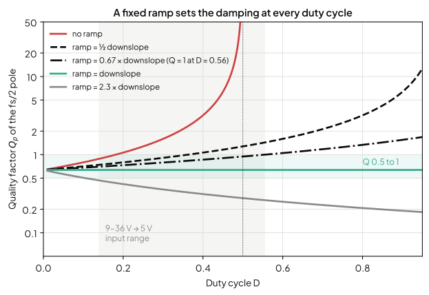
On this converter the three input corners read:
| Ramp | 9V (D = 0.56) | 18V (D = 0.28) | 36V (D = 0.14) |
|---|---|---|---|
| ½ × downslope | 1.43 | 0.88 | 0.74 |
| 0.67 × downslope | 1.00 | 0.78 | 0.70 |
| 1 × downslope | 0.64 | 0.64 | 0.64 |
| 2.3 × downslope | 0.26 | 0.37 | 0.47 |
What too little ramp costs
Fig. 2 designs a Type II at 18V for each of two ramps, then measures it at all three corners without changing it. On the left the ramp is half the downslope. On the right it is the full downslope.
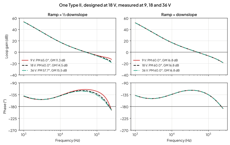
With half the downslope, gain margin runs 11.3, 14.5 and 15.5dB from 9V to 36V. Phase margin runs 65.0°, 60.0° and 57.7°. The worst gain margin and the worst phase margin sit at opposite ends of the input range.
That split caught me out. One of the reference designs in switchmode.io is a 19.2–28.8V to 5V buck. Its worst gain margin, 4.99dB, was at minimum input. Its worst phase margin, 39.7°, was at maximum input. Its ramp was 0.35 times the downslope.
At low input the duty is highest, is highest and the peaking at eats the gain margin. At high input is lowest, and the lower-Q pole puts more phase lag in at crossover. Checking one end of the range and passing tells you nothing about the other.
On this converter the spread is 7° and 4dB. That is real, but it isn't a disaster. The dramatic numbers are at the two extremes, no ramp and too much.
What too much ramp costs
More ramp lowers , and a lower-Q pole at starts taking phase at lower frequencies. That matters at the crossover frequency , which Parts 1 and 2 set at , or 50kHz.
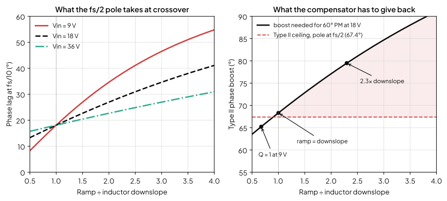
With the ramp equal to the downslope, the pole takes 18.1° at a crossover of . At 2.3 times the downslope it takes 38.6° at 9V. That phase has to come back from somewhere.
A Type II compensator can't give it all back. With its pole held at , it can deliver at most , which is 67.4° at . I work through where that ceiling comes from in Compensator Types: Choosing Between Type I, II and III. Against it:
| Ramp | Boost needed at 18V | Against the 67.4° ceiling |
|---|---|---|
| ½ × downslope | 63.5° | fits |
| 0.67 × downslope | 65.2° | fits |
| 1 × downslope | 68.3° | 0.9° short |
| 2.3 × downslope | 79.5° | 12° short |
| 4 × downslope | 91.1° | impossible for any Type II |
So the ramp most references call optimal is slightly beyond what a Type II can deliver at and 60°. You can lower the crossover, accept less phase margin or move to a Type III. That is Sheehan's point that "the only performance drawback with too much slope compensation is a lower crossover frequency" [4, p. 25]. It's right about the loop, but the lower crossover isn't free.
There are legitimate reasons for more ramp than the downslope. Erickson notes that noise on the sense signal can call for a ramp "substantially greater than the inductor current ripple" [2, pp. 448–449]. The cost above is what you pay for that margin.
Whether it costs load current depends on your part
On some controllers extra ramp also costs output current. On others it doesn't, and the datasheet tells you which.
The TI LM5088 applies its emulated current signal, ramp included, "to the current limit comparator" [8, §7.3.8]. Its sense-resistor equation leaves headroom for the recommended ramp and no more. Sized by its own equations for this converter, the ramp matches the downslope and 2A is delivered at every input. At three times the downslope, the minimum current-limit threshold gives 1.95A against the 2.15A peak needed at 9V. At four times it fails at the typical threshold too.
That isn't universal. The TI LM5141 senses its limit on a separate comparator [9, §7.3.9]. The TPS54360B clamps the error amplifier too. Its datasheet says the limit "is not affected by the slope compensation and remains constant over the full duty cycle range" [10, §7.3.2]. Linear Technology's LT1339 avoids it with an average current limit [7, p. AN73-18]. Check the current-limit section of your datasheet before you add ramp.
So how much ramp?
Size a fixed ramp for of about one at the highest duty cycle you run, then check the other end of the range. That is Ridley's rule [5]. It works out as . At this converter's maximum duty of 0.556, that is 0.67 times the downslope.
On the same converter, with the Type II redesigned for it:
| 9V | 18V | 36V | |
|---|---|---|---|
| 1.00 | 0.78 | 0.70 | |
| Phase margin | 63.1° | 60.0° | 58.5° |
| Gain margin | 13.7dB | 15.3dB | 15.9dB |
The spread is 4.6° and 2.2dB. It needs 65.2° of boost, which a Type II can deliver. On this converter it's a better trade than the full downslope. That buys identical corners, but at the price of a compensator that can't quite reach its target.
Use the full downslope when you can afford its phase. That usually means a crossover below or a Type III. Its flat pays for itself on a very wide input range.
Whichever you pick, remember that the ramp is fixed and the inductor isn't. Set the ramp to the nominal downslope and let the inductance fall to 70%, from tolerance or soft saturation at peak current. at 9V moves from 0.64 to 0.96. The invariance is exact only at nominal inductance. I cover tolerance effects on the loop in Worst-Case Phase Margin: What Component Tolerance Does to Your Buck Converter.
Valley current mode turns the problem over
Valley current mode is the mirror image. The clock turns the switch off, and the comparator turns it on when the current falls to the threshold. It rides the downslope and needs a ramp below 50% duty rather than above it [4, p. 5]. The ramp is sized against the on-slope instead.
On a buck the on-slope is , and that does move with input voltage. On this converter it changes by a factor of 7.8 across the range. So no fixed ramp gives valley mode the invariance peak mode gets for free:
| Valley ramp | 9V | 18V | 36V |
|---|---|---|---|
| none | = 5.7 | unstable | unstable |
| ½ × on-slope at 36V | 0.18 | 0.50 | 4.6 |
| 1 × on-slope at 36V | 0.09 | 0.21 | 0.64 |
The half-slope rule, sized at the worst corner, leaves at 4.6 there and 0.18 at the other end. Renesas makes the general point that "fixed slope compensation cannot handle all duty cycles and inductors" [11, p. 4]. Its ISL8117 valley-mode controller adapts its ramp to input voltage [11, p. 5].
Applying this to a design
The ramp is a loop design parameter, not a stability patch. Treat it like one. Three checks follow from everything above:
- Work out at both ends of the input range, not just at nominal.
- Read the phase your chosen crossover loses to the pole, and check your compensator type can return it.
- Check whether your part's current limit sees the ramp.
The numbers here come from Ridley's small-signal model, on the same converter as Parts 1 and 2. They are one converter, not a survey.
Doing this properly on a real design means reading every margin at every input corner. It means using the ramp your controller actually applies, and the inductance it actually has at peak current. That is the analysis switchmode.io is being built to do. It grades loop margins at every corner of the input range and names the worst one. A margin is a reading at an operating point, not a property of the design.
References
[1] R. B. Ridley, "A New Small-Signal Model for Current-Mode Control," Ph.D. dissertation, Virginia Polytechnic Institute and State University, Blacksburg, VA, USA, 1990. [Online]. Available: https://ridleyengineering.com/images/current_mode_book/CurrentModeControl.pdf
[2] R. W. Erickson and D. Maksimović, "Current programmed control," in Fundamentals of Power Electronics, 2nd ed. Norwell, MA, USA: Kluwer Academic, 2001, ch. 12, pp. 439–487.
[3] Unitrode, "Modelling, Analysis and Compensation of the Current-Mode Converter," Application Note U-97, Texas Instruments SLUA101. [Online]. Available: https://www.ti.com/lit/pdf/slua101
[4] R. Sheehan, "Understanding and Applying Current-Mode Control Theory," Texas Instruments SNVA555, 2007. [Online]. Available: https://www.ti.com/lit/pdf/snva555
[5] R. B. Ridley, "Current-Mode Control Modeling," Switching Power Magazine, 2006. [Online]. Available: https://ridleyengineering.com/images/pdf-design_center/5-current-mode-control-modeling.pdf
[6] C. Nelson, "LT1070 Design Manual," Application Note 19, Linear Technology, Jun. 1986. [Online]. Available: https://www.analog.com/media/en/technical-documentation/application-notes/an19fc.pdf
[7] D. Eagar, "LT1339 Design Manual," Application Note 73, Linear Technology, Feb. 1999. [Online]. Available: https://www.analog.com/media/en/technical-documentation/app-notes/an-73f.pdf
[8] Texas Instruments, "LM5088, LM5088-Q1 Wide Input Range Non-Synchronous Buck Controller," SNVS600J, Jun. 2022. [Online]. Available: https://www.ti.com/lit/ds/symlink/lm5088.pdf
[9] Texas Instruments, "LM5141 Wide Input Range Synchronous Buck Controller," SNVSAU0, Mar. 2017. [Online]. Available: https://www.ti.com/lit/ds/symlink/lm5141.pdf
[10] Texas Instruments, "TPS54360B 4.5-V to 60-V Input, 3.5-A Step-Down DC-DC Converter," SNVSB93, Dec. 2018. [Online]. Available: https://www.ti.com/lit/ds/symlink/tps54360b.pdf
[11] Renesas Electronics, "How to Select a PWM Controller for Narrow On-Time Buck Conversion," white paper. [Online]. Available: https://www.renesas.com/en/document/whp/how-select-pwm-controller-narrow-time-buck-conversion